[Documenting the happy outcome]
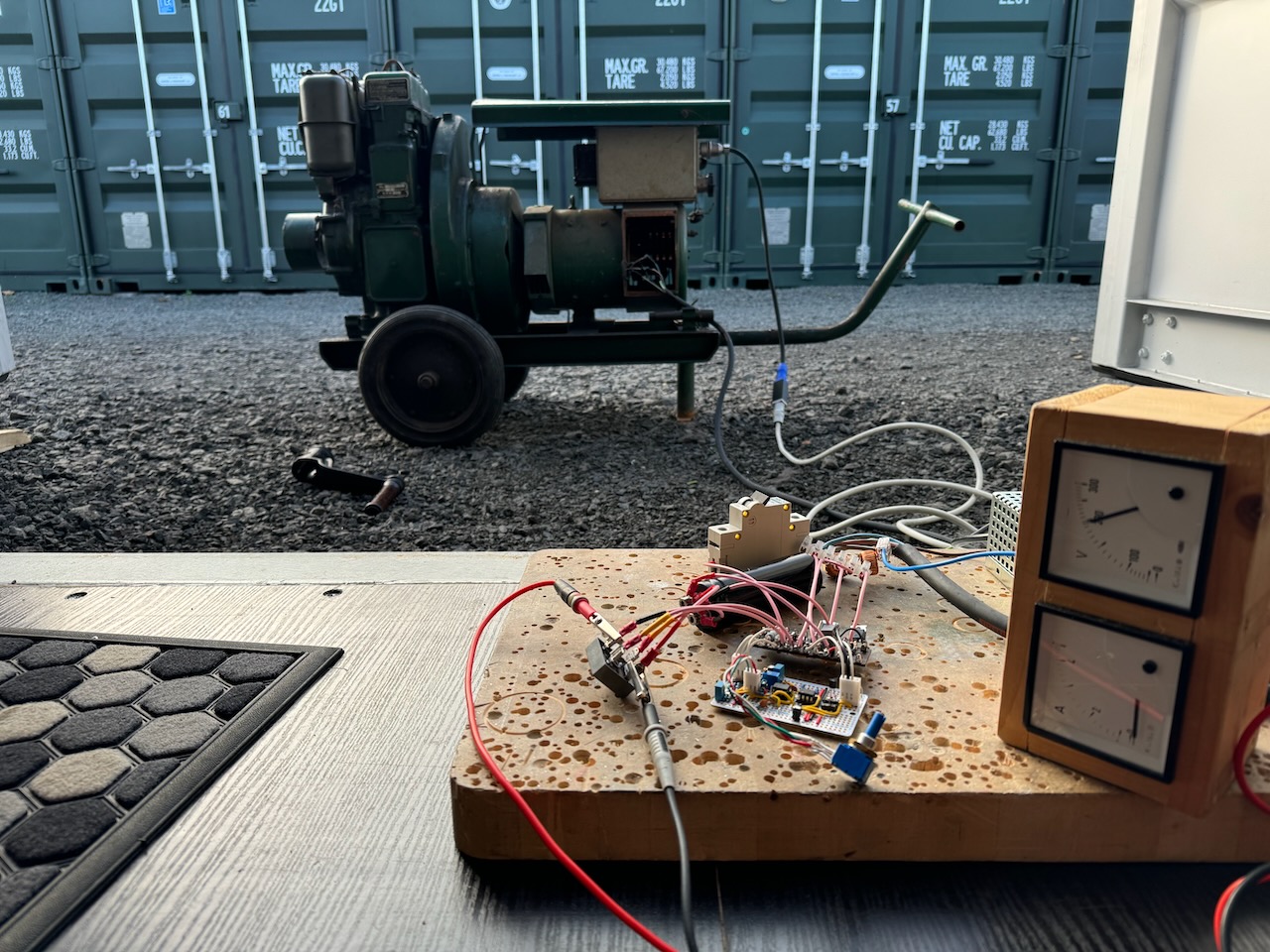
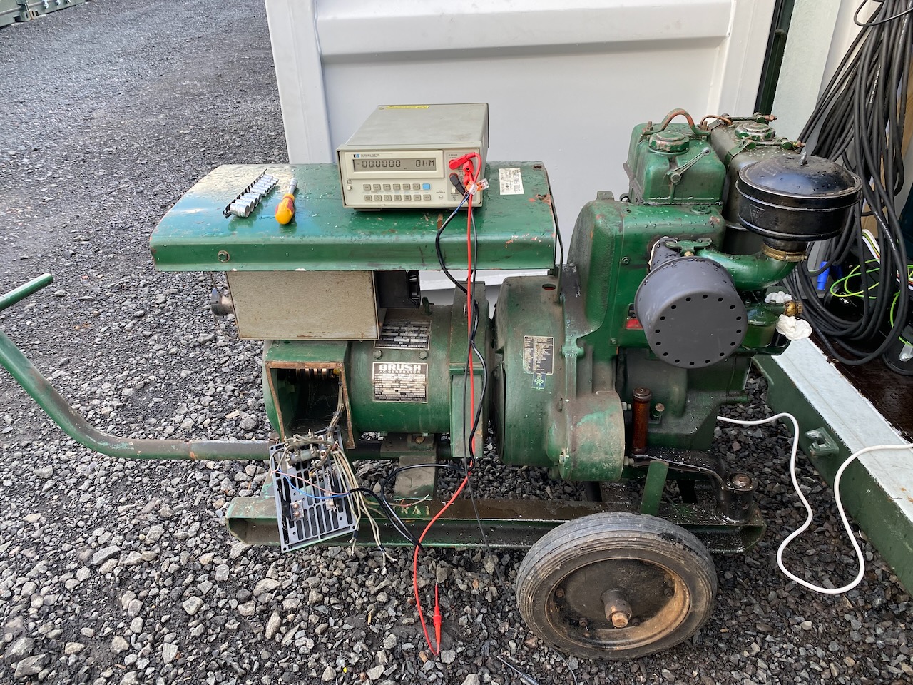
This was a long-running project to get my welder running off the Lister diesel generator. After a few dead ends it is now officially finished and has become a piece of workshop equipment for day-to-day welding of other things.
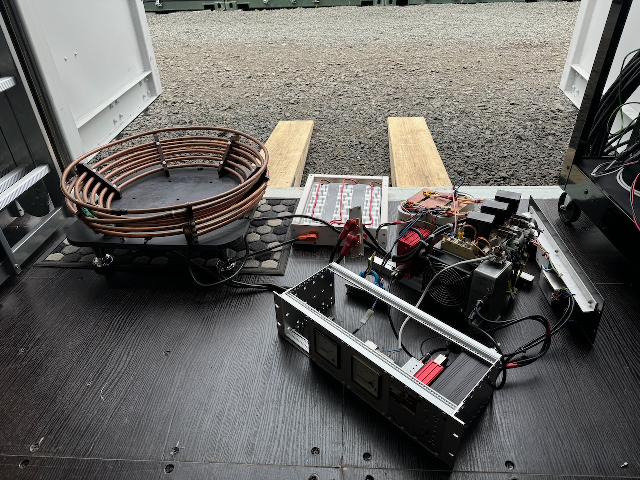
It ended up split into two sections which I’ll call the Happy Welder 3000S and 3000T. The division was a bit arbitrary and was really about letting me reuse salvaged enclosures from my junk heap.
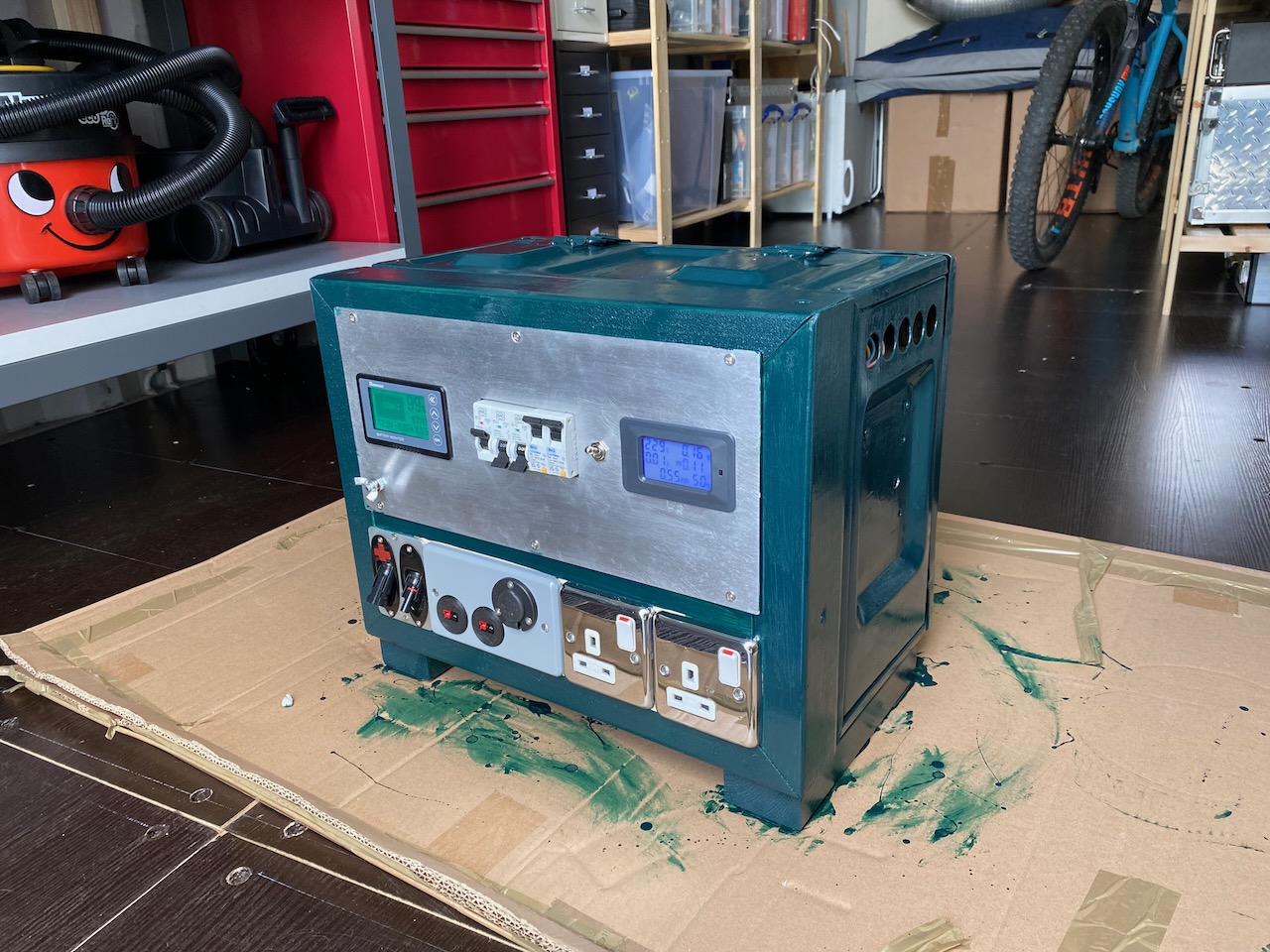
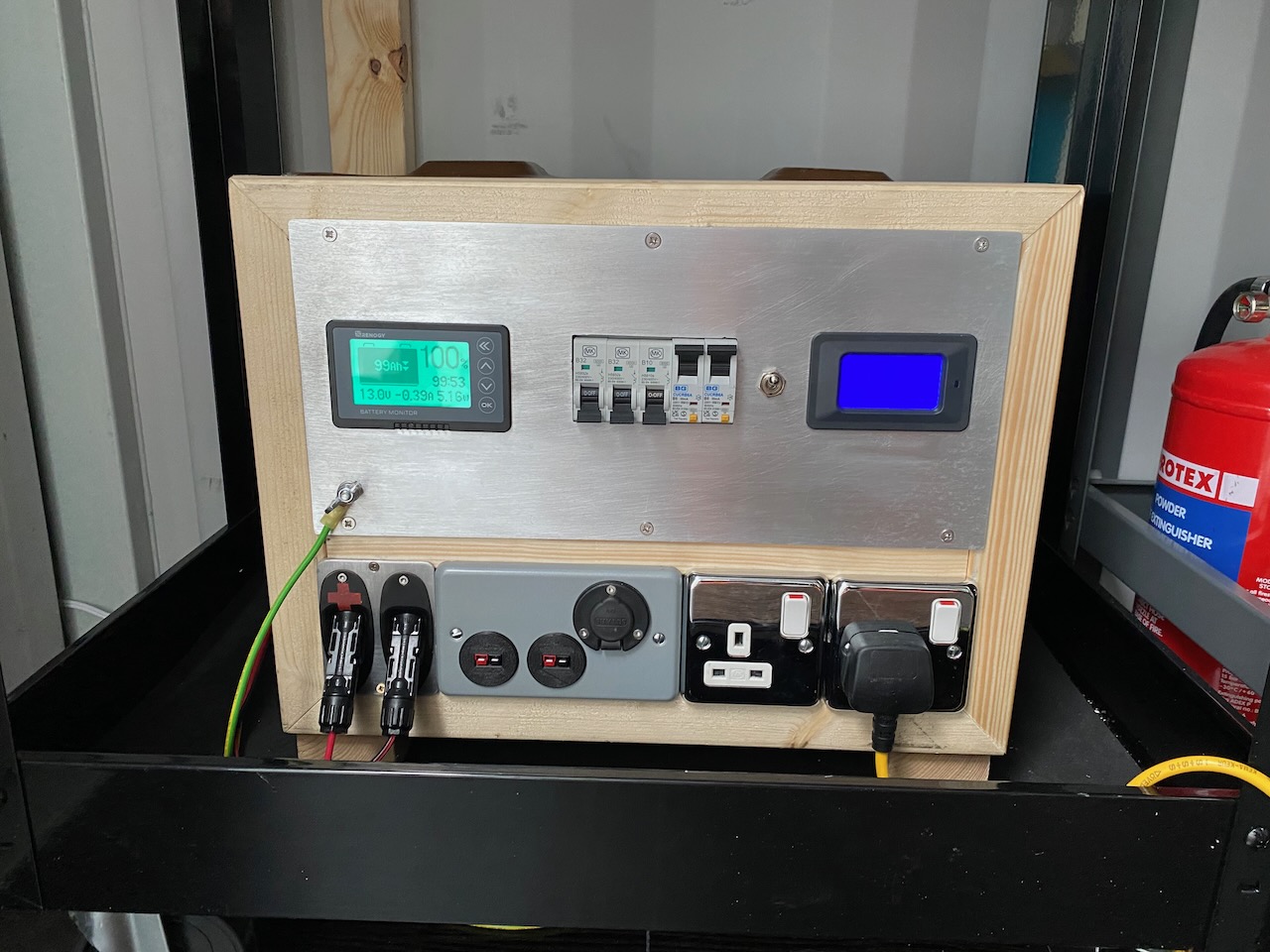
Happy Welder 3000S
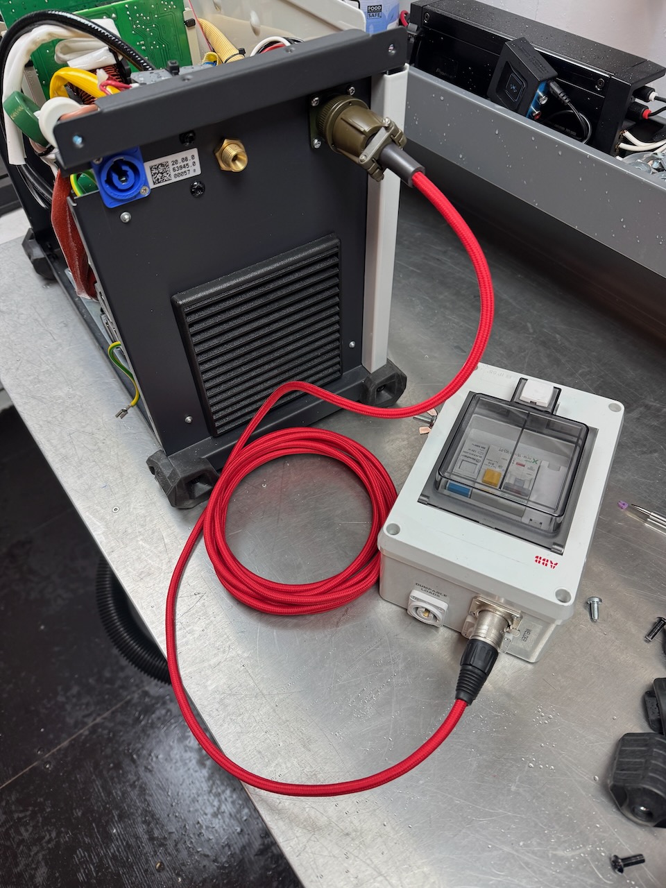
The “S” stands for switch box or splitter. The main purpose of this part is to split the incoming supply from the generator into two. One feed goes to the welder and the other to a selection of “dumpable loads” which are switched off while welding is in progress.
The motivation behind this is to keep a decent amount of load on the engine most of the time. Diesels like to work and will get clogged up with soot if left idling for long periods of time. And the nature of welding is short periods of high power draw with long breaks in between. (at least at Container Labs it is, I’m not planning on building a ship any time soon)
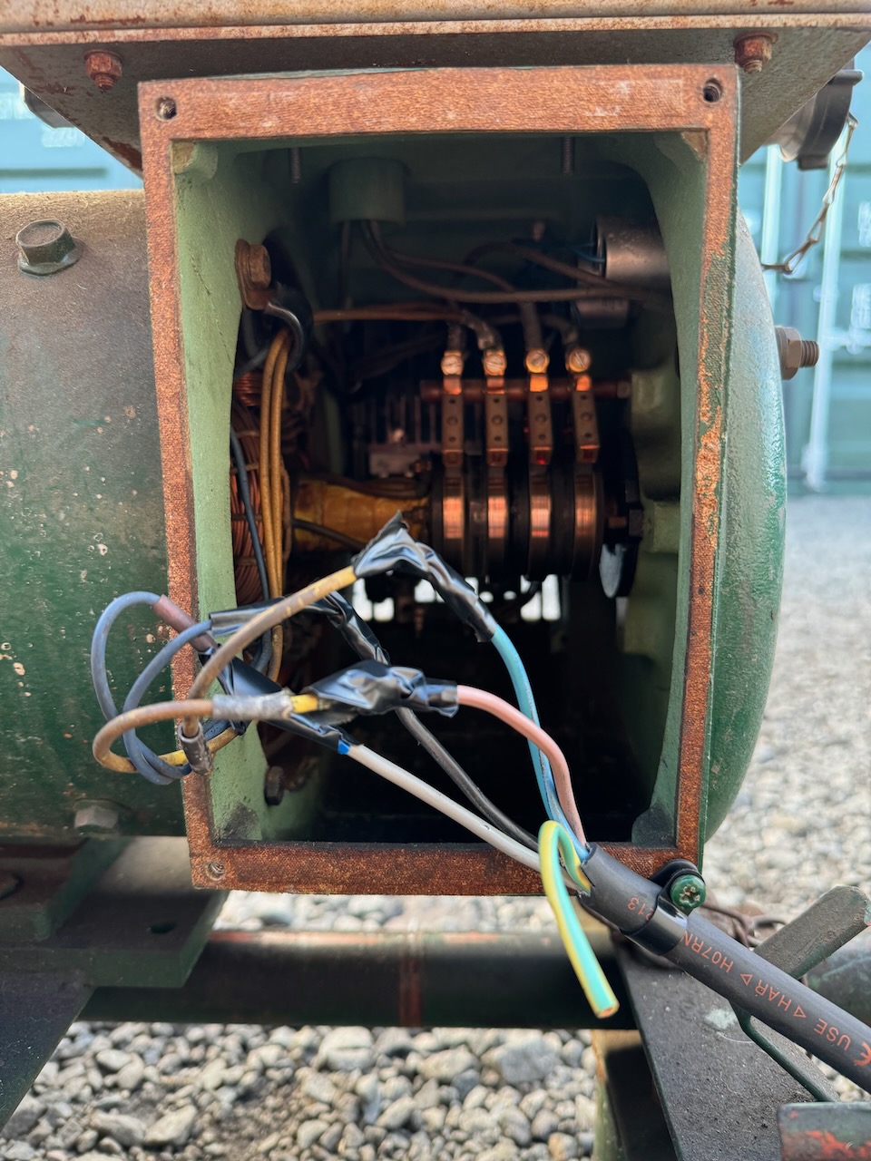
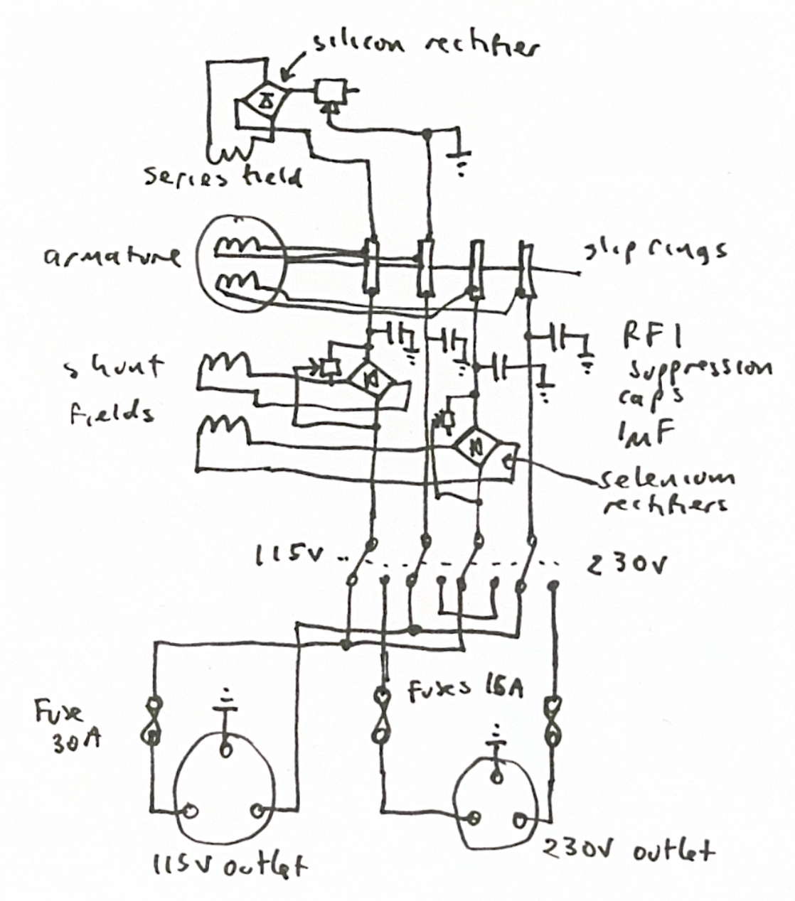
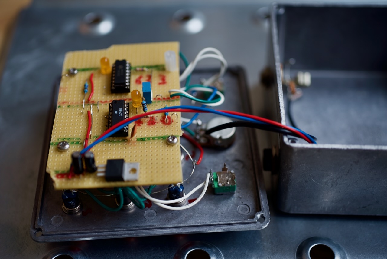
I fiddled with a few different schemes to turn off the dumpable loads by sensing the supply current draw of the welder, but couldn’t get this to work reliably. So I modified the welder slightly. It has a solenoid operated gas valve inside that supplies argon to the torch while welding. This opens a second or two before the arc is struck and stays open for about 20 seconds after it goes out. Just perfect for actuating a load dump contactor.
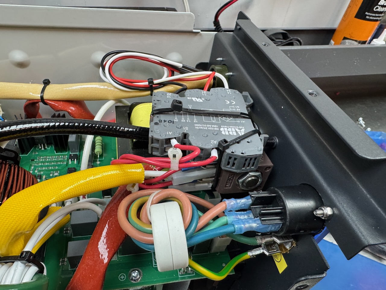
Using some zip ties and piggyback spade terminals, I connected a relay in parallel with the gas valve operating coil. This runs off 24V DC so finding a suitable relay was no problem. To save drilling a hole* in the welder I repurposed the 3 unused pins on the foot pedal connector. I do have a foot pedal, but it plugs into the hand controller socket on the front panel.
* another hole- the eagle-eyed might notice that I’ve already replaced the captive power cord with a Neutrik Powercon inlet. I love Powercons 😀
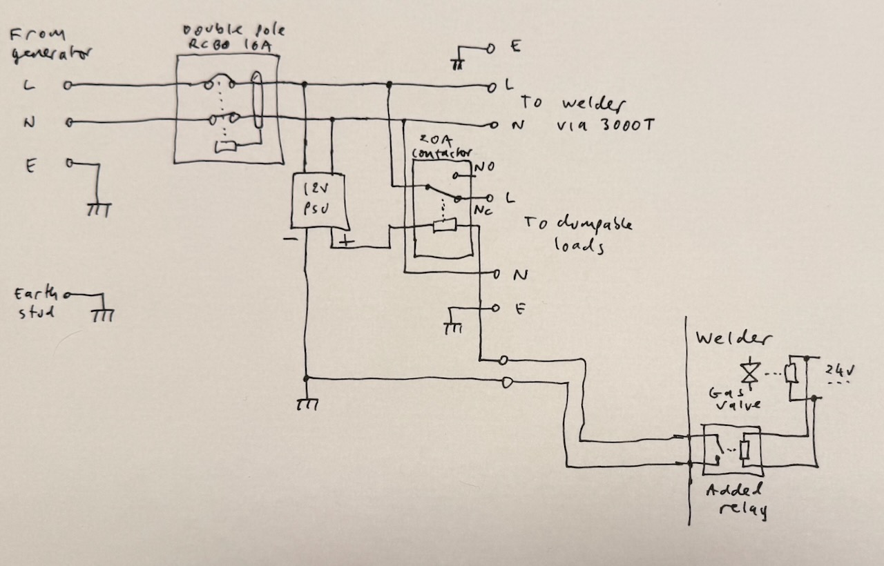
I wanted a low voltage signal for triggering the load dump contactor. The relay I added inside the welder is quite capable of switching 230V, but the foot switch plug has male pins that could deliver an electric shock when unplugged if I used mains voltage here. So the finishing touch was a small low voltage power supply inside the 3000S enclosure just for the contactor coil. I used a 12V switched mode wall wart with the pins trimmed down and a piece of plastic attached with hot glue to insulate the stumps.
The CPC catalogue turned up an inexpensive 20A contactor with a 12V coil and normally closed contact, and the 3000S was done.
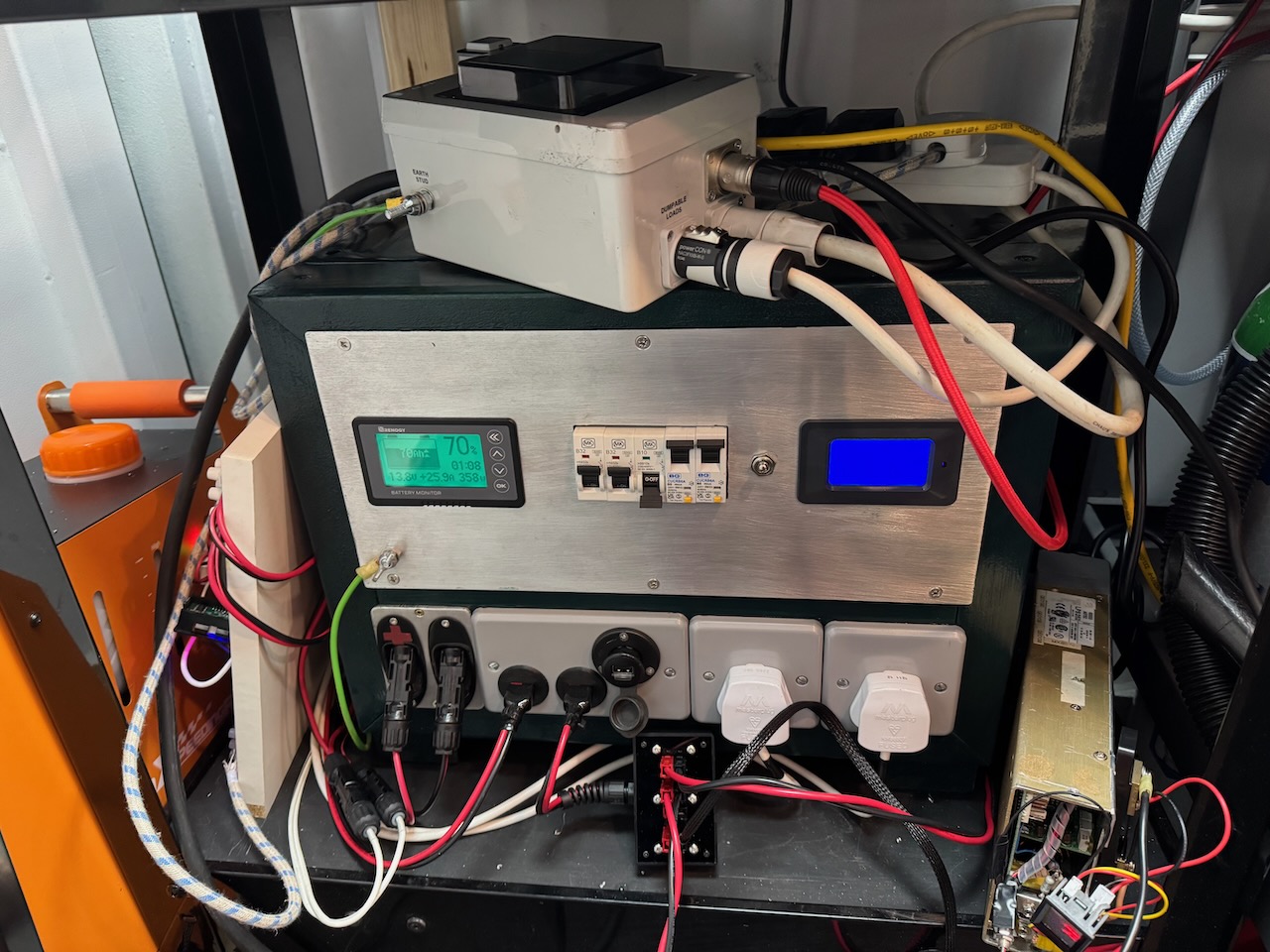
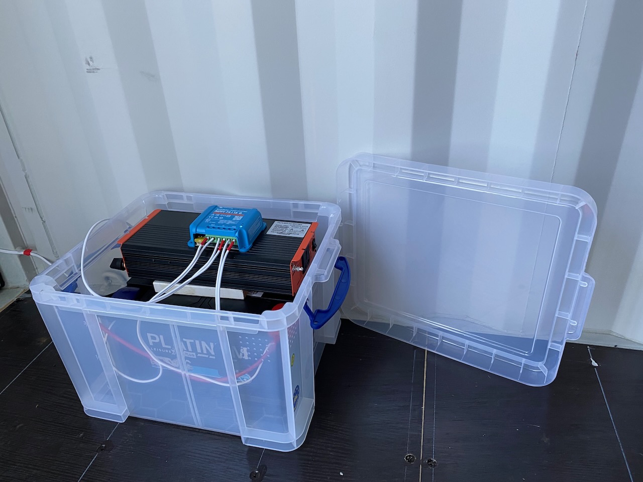
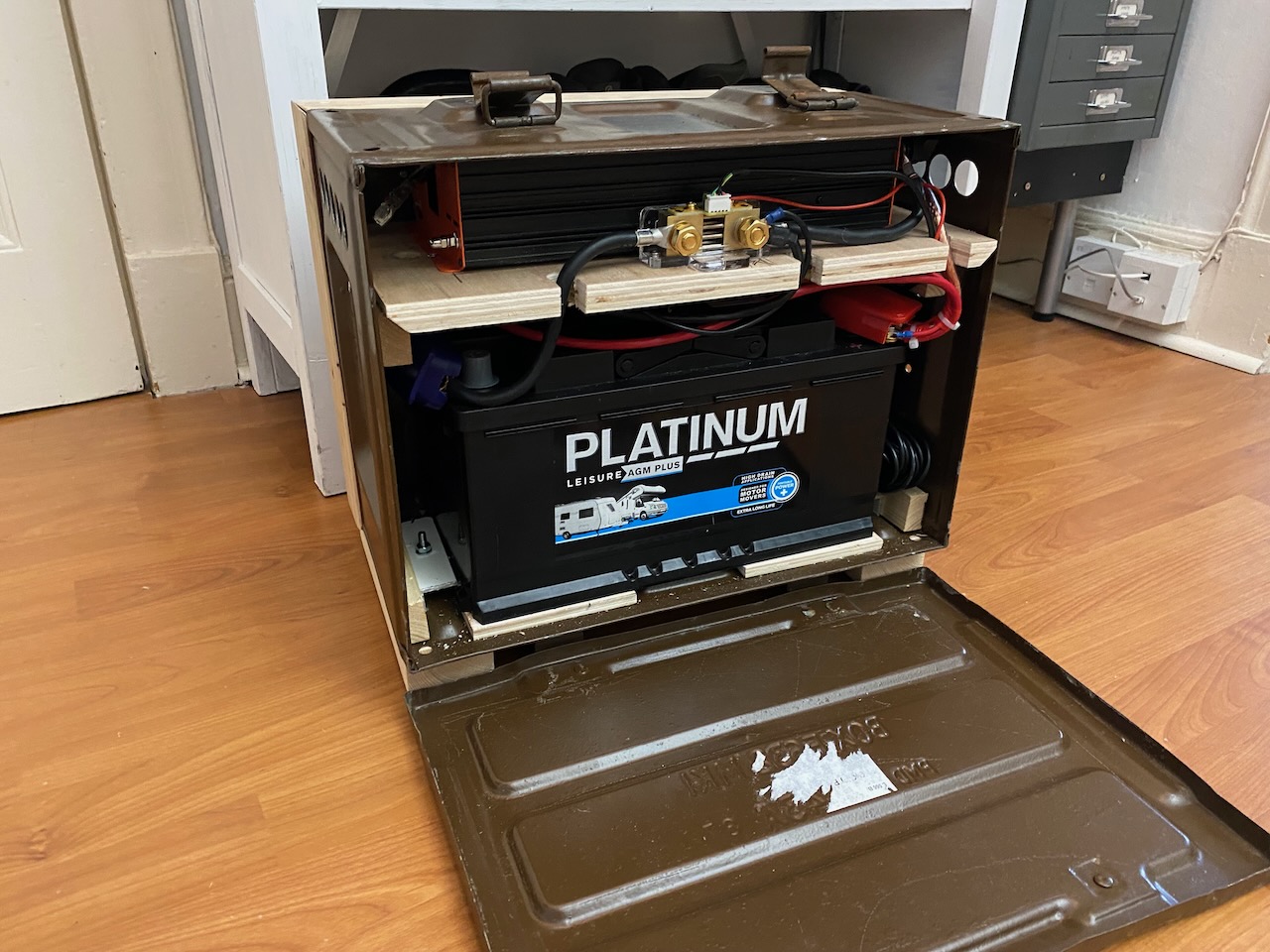
In use the “dumpable loads” are two battery chargers feeding the Power Tank, and an electric heater. The 3000S also serves as the earthing point for the generator and everything connected to it.
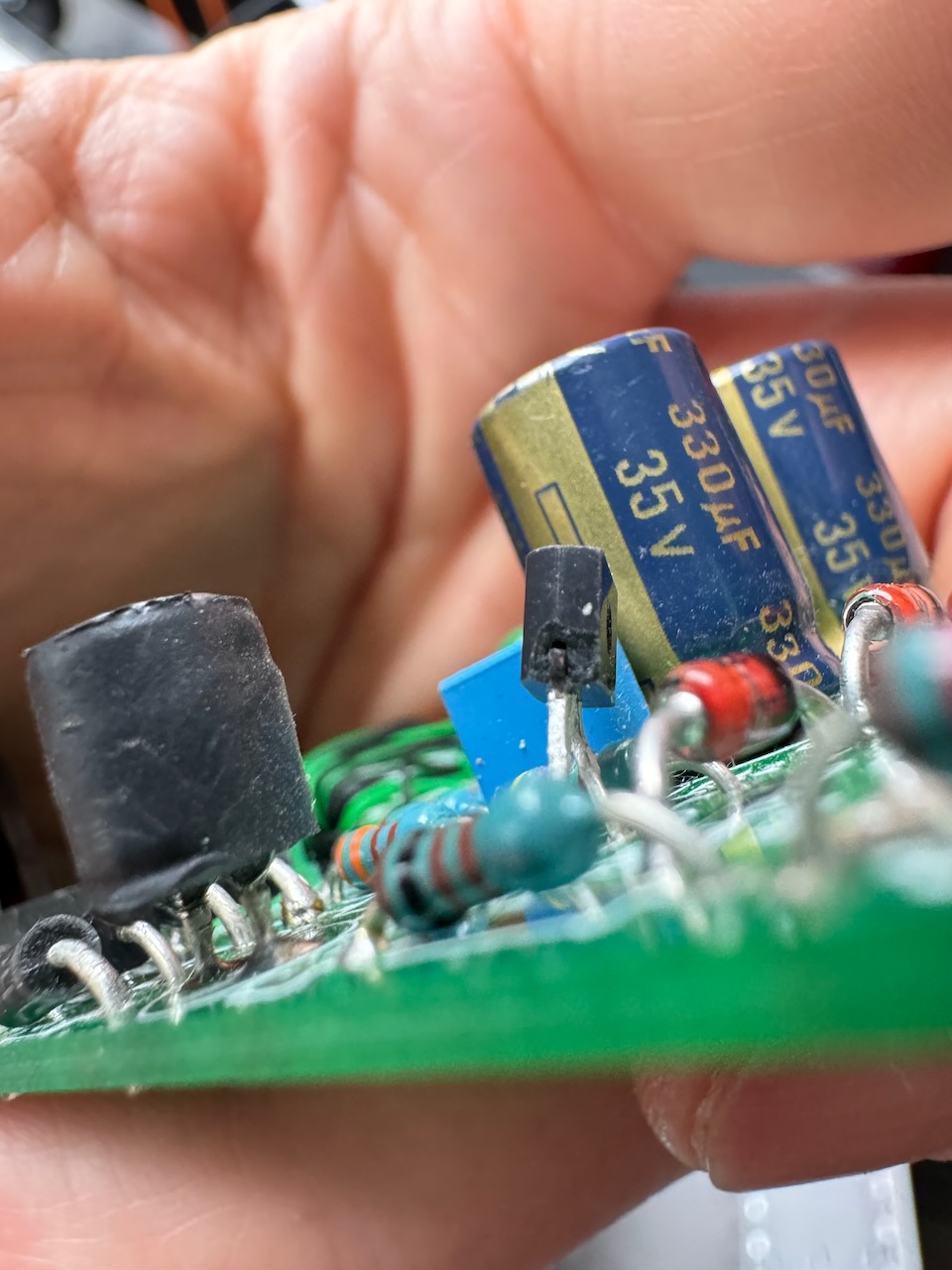
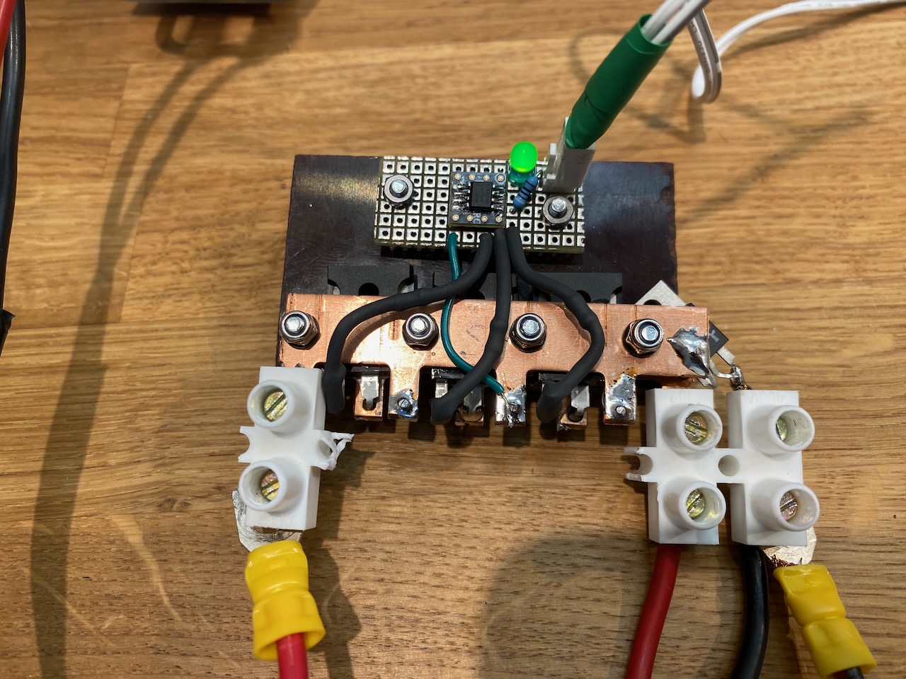
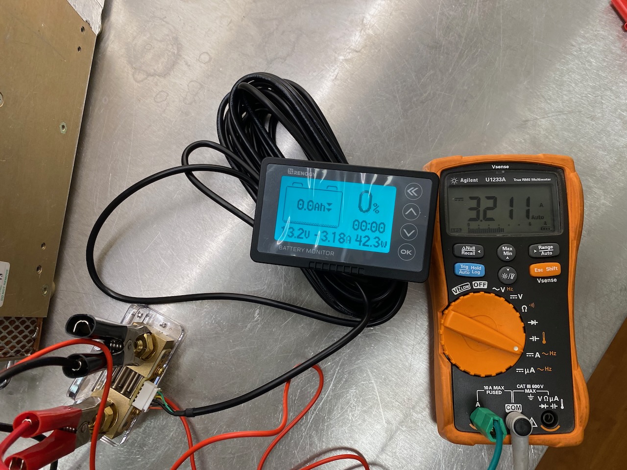
The battery chargers are modified switched mode power supplies which I’ll write about another time. In the bottom right you can see my long-suffering Astec LPS250 which started life as 5V, 50A, and is now cranking out 30A at 14.4V. Not bad for a “250W” unit, do I smell burning? :/
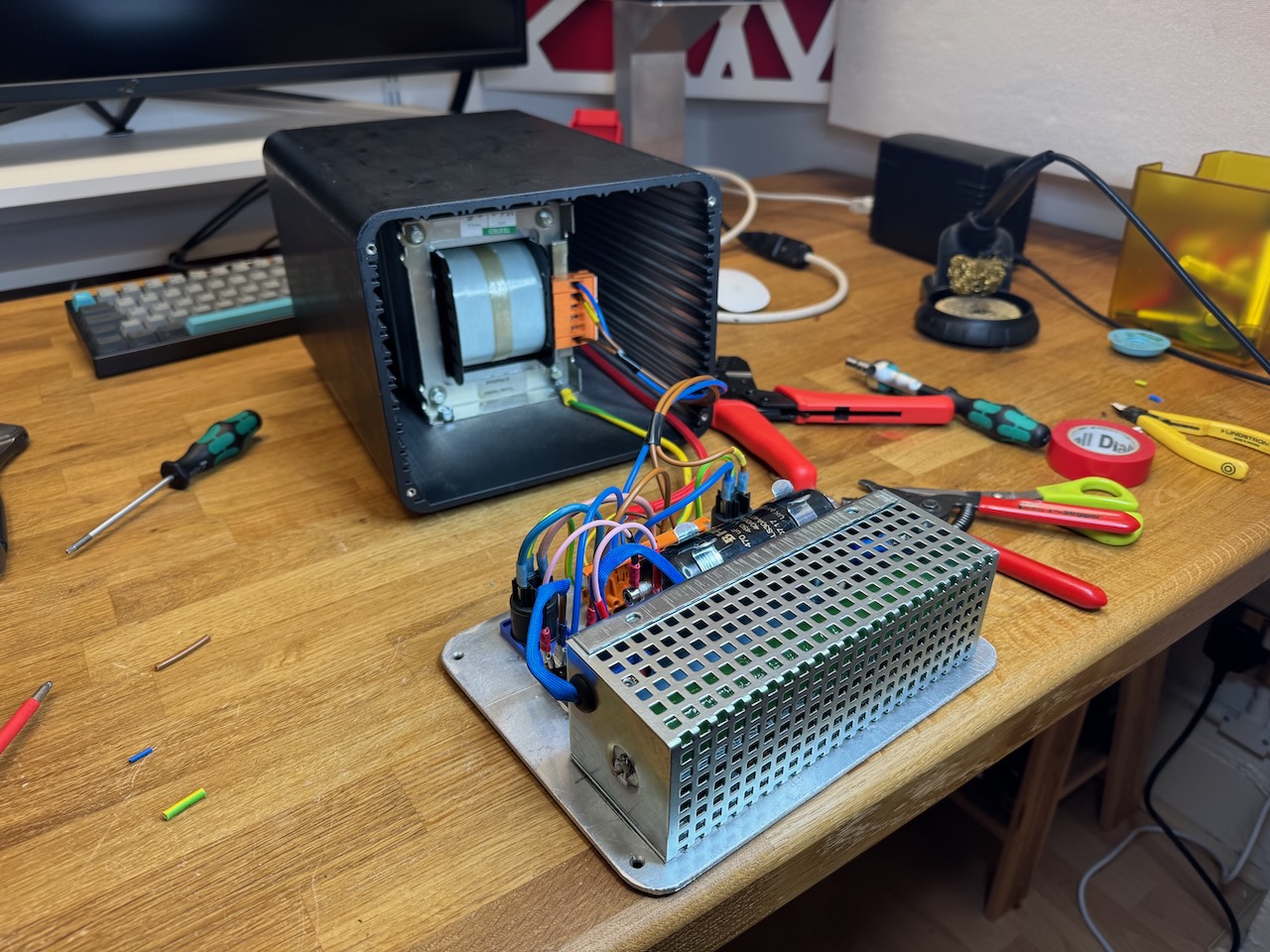
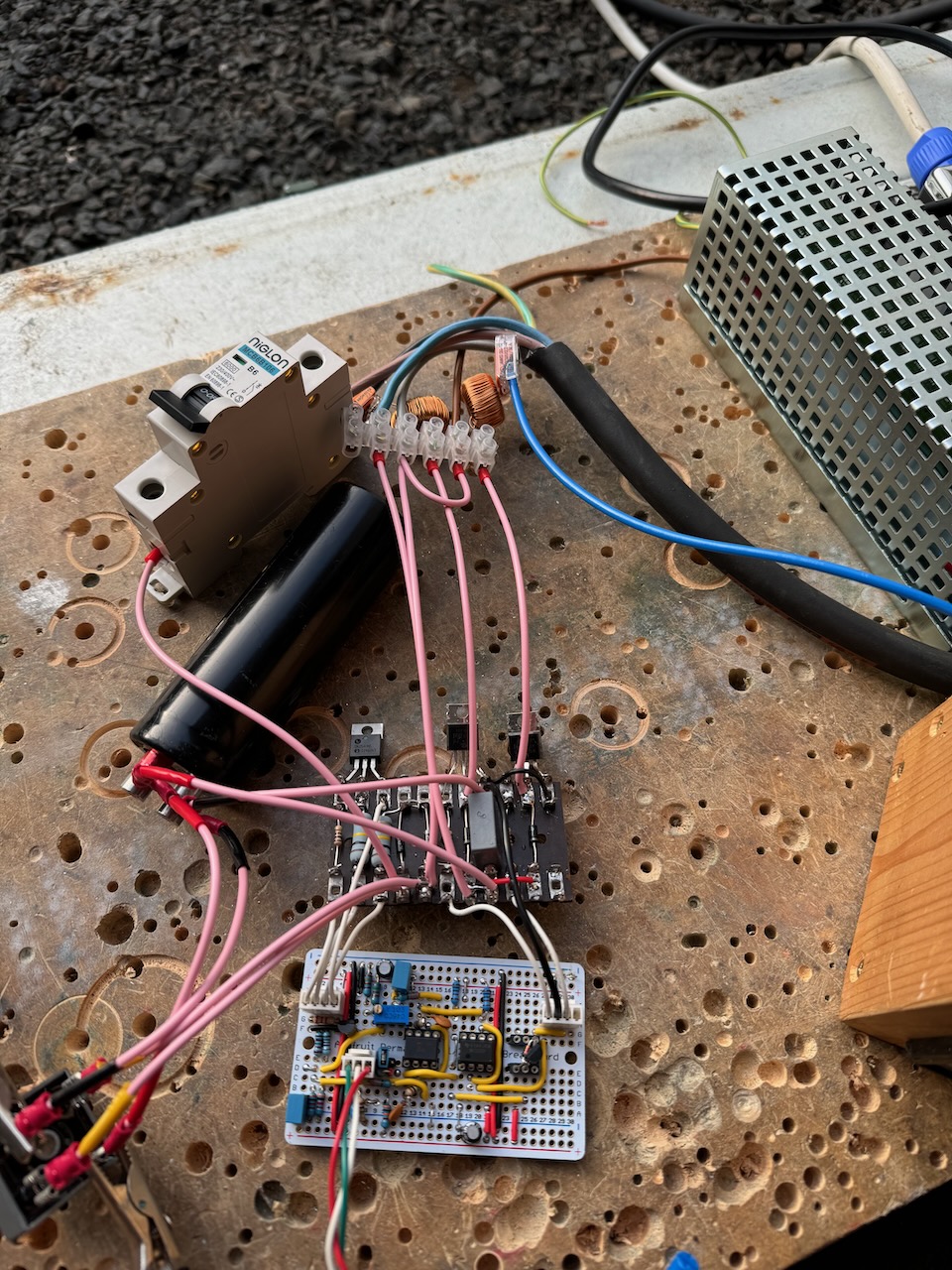
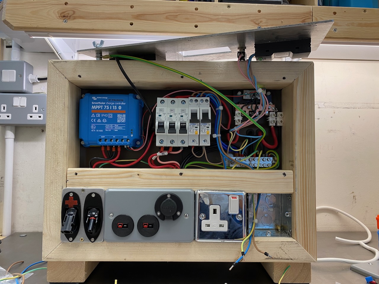
Happy Welder 3000T
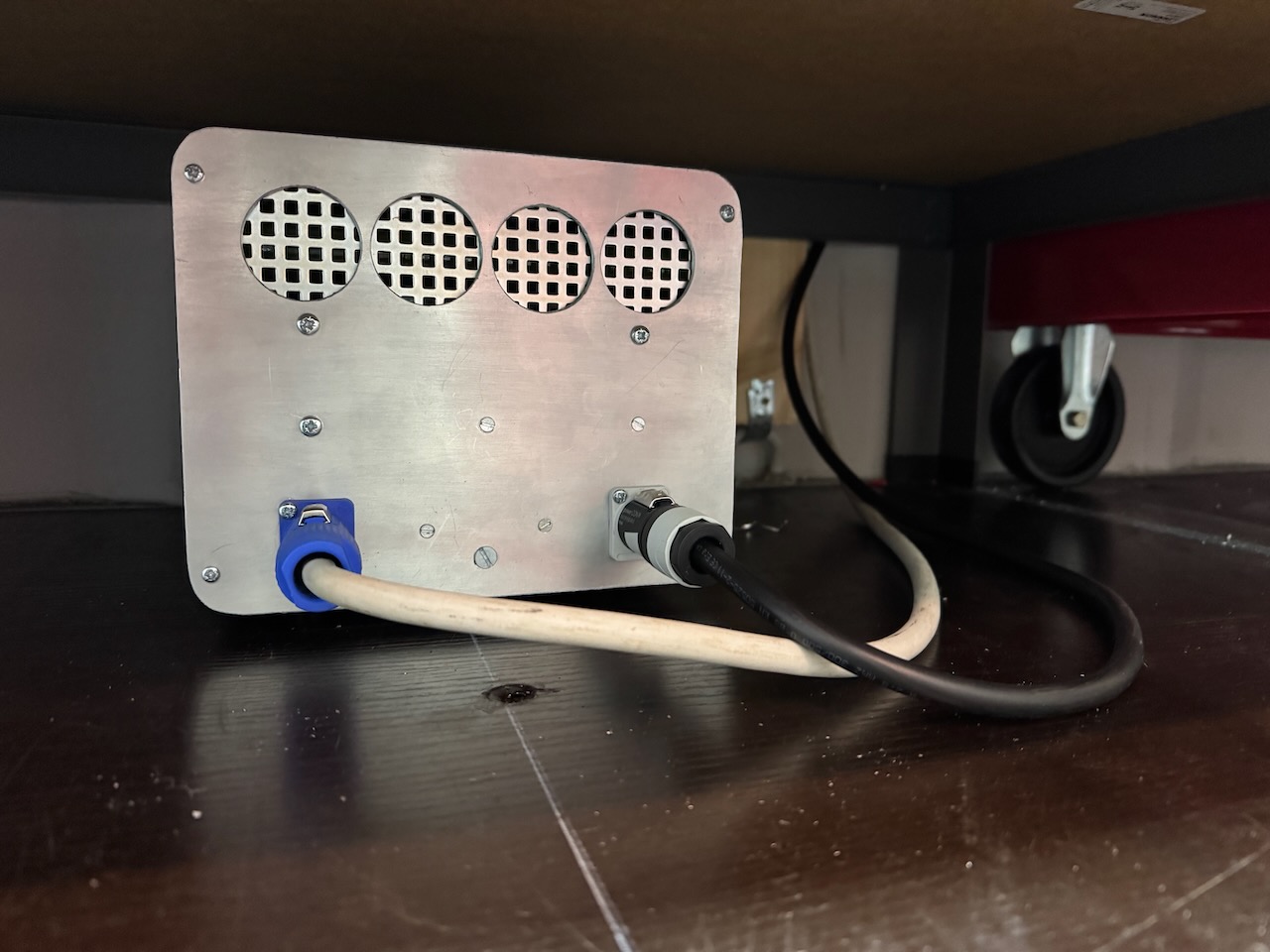
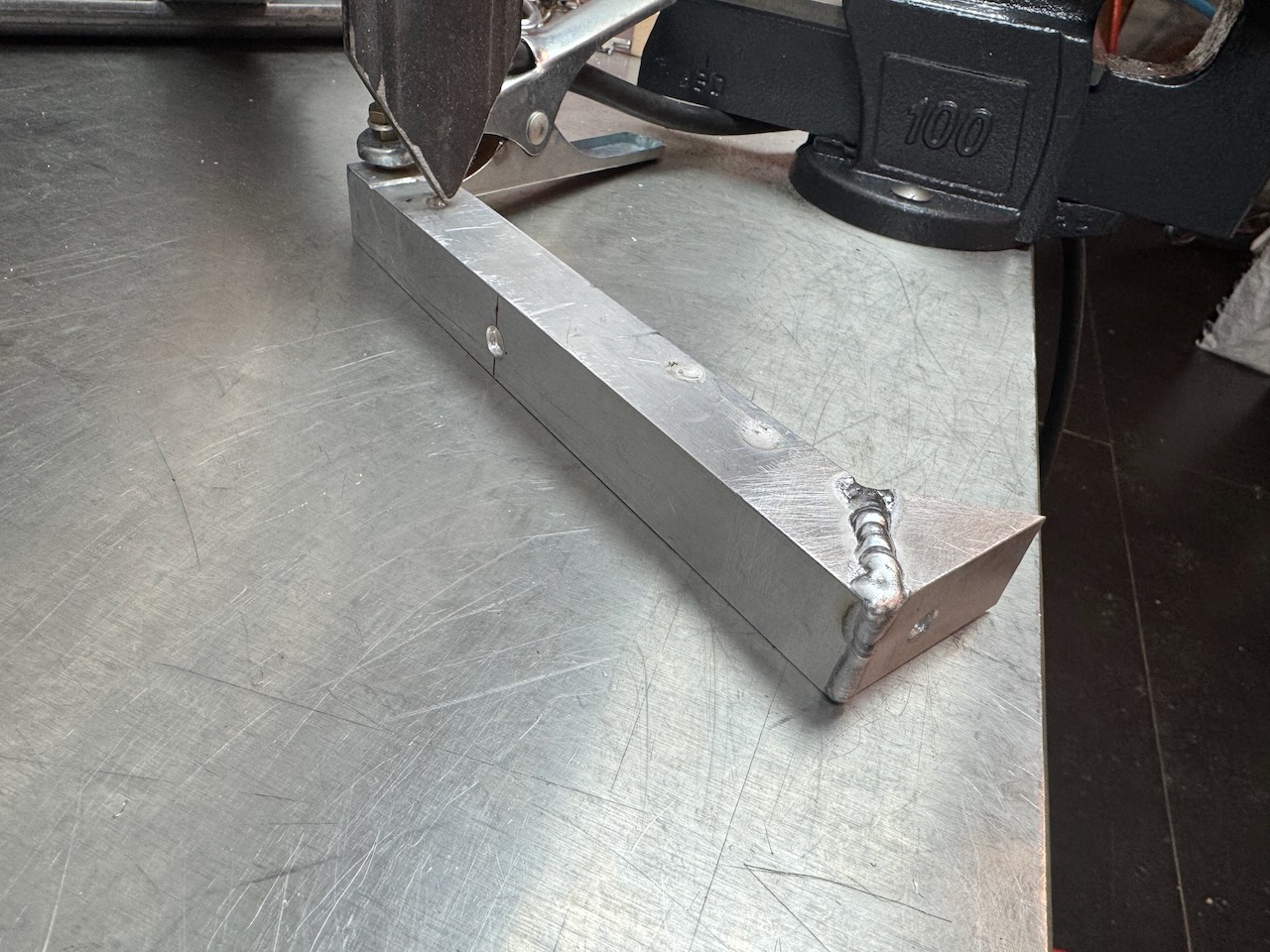
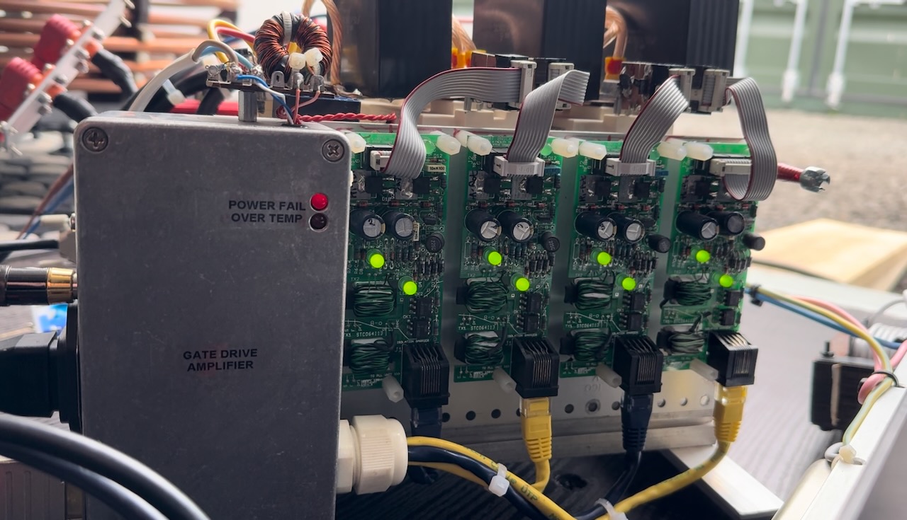
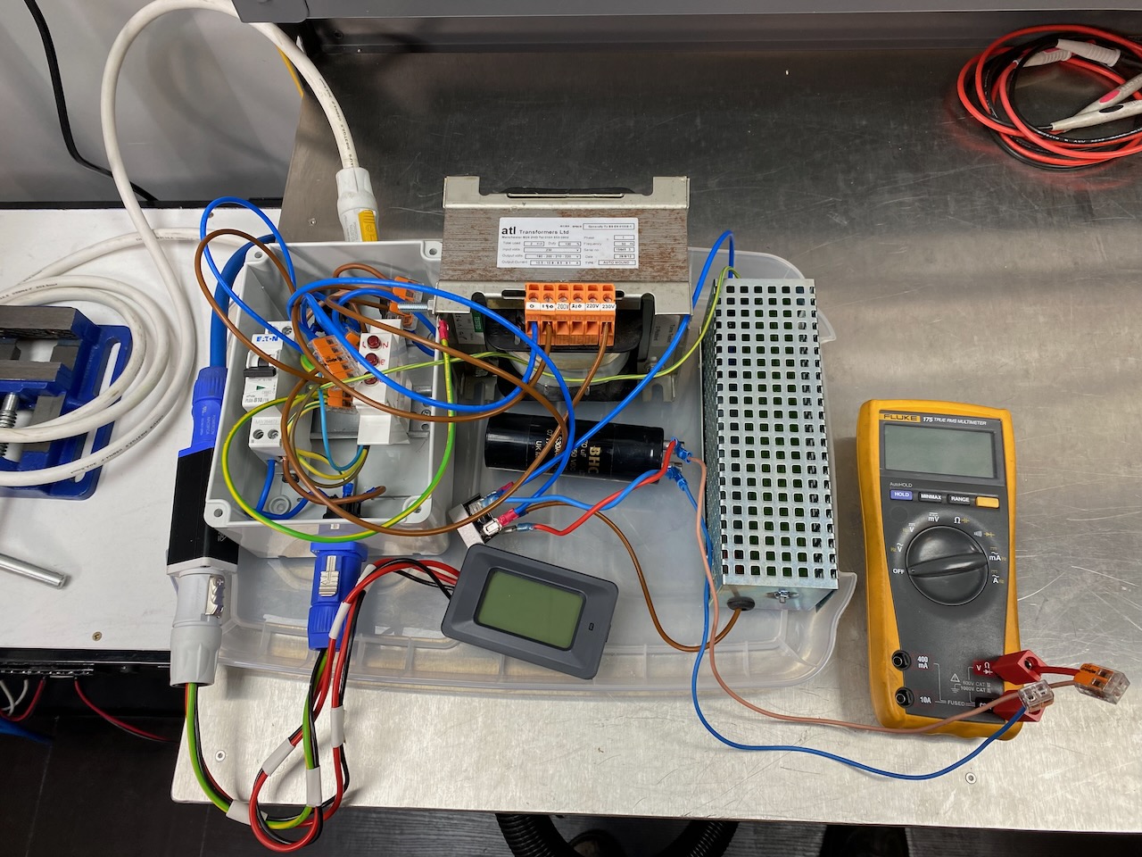
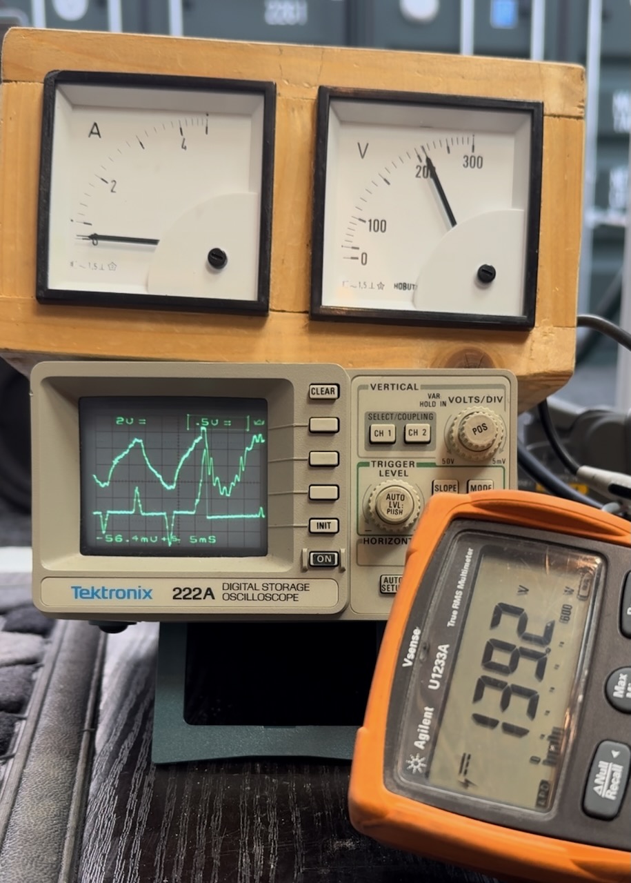
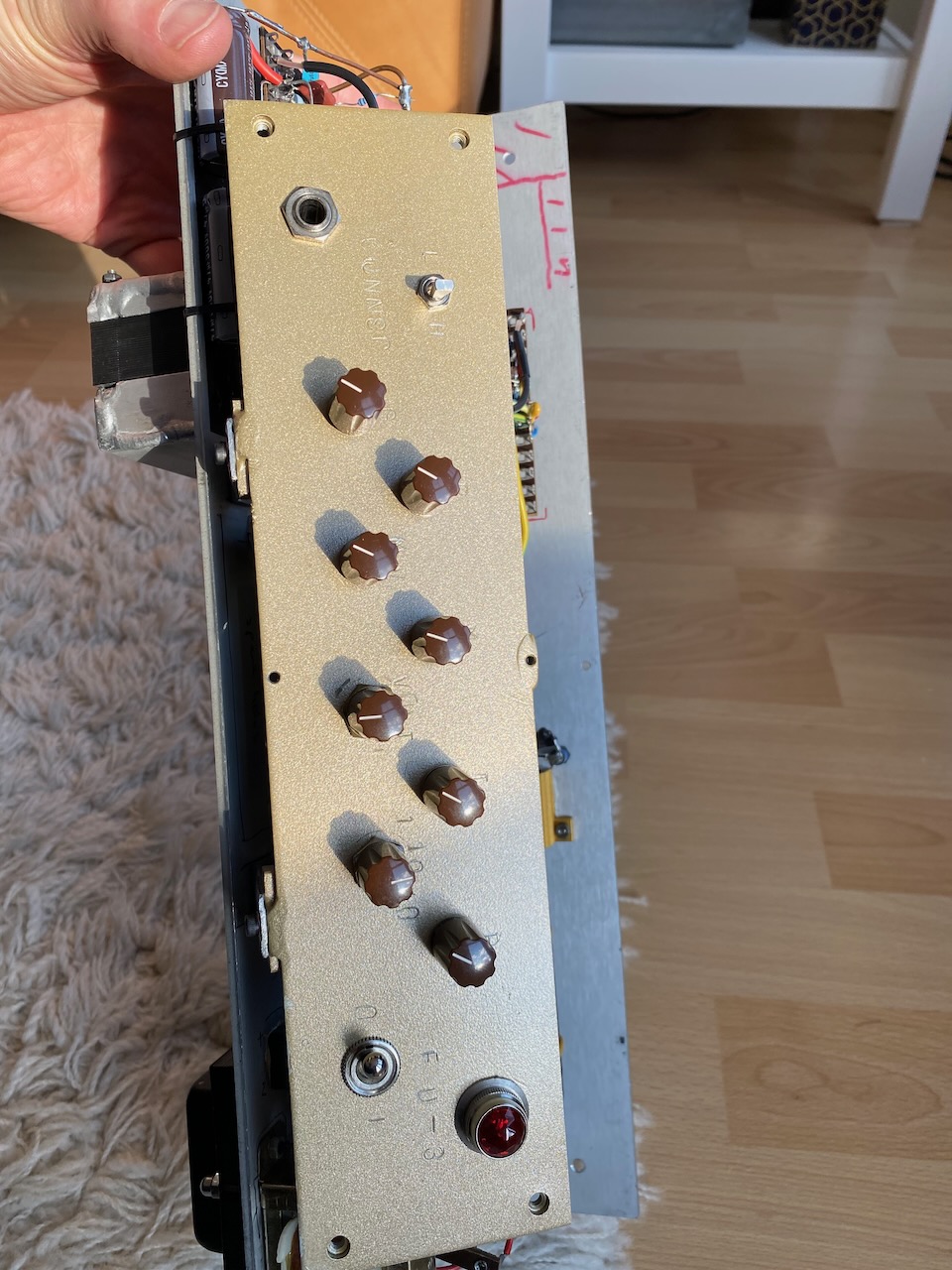
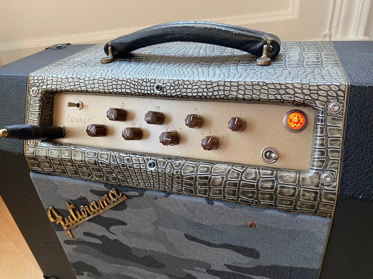
T is for transformer. This box (a Pentium 4 PC in a previous life) contains all of the parts that I found were needed to make the welder accept Lister’s quirky retro power quality. I already had this enclosure in my junk pile and it fitted perfectly under the workbench. I pondered trying to squeeze the 3000S parts in here too but decided it would be a wiring and assembly nightmare.
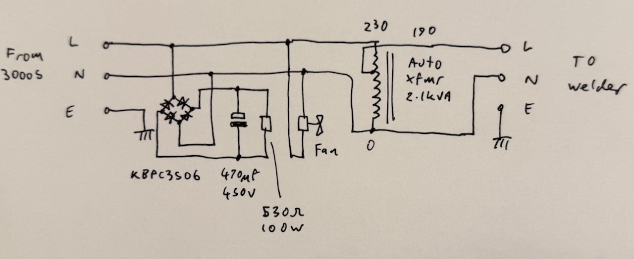
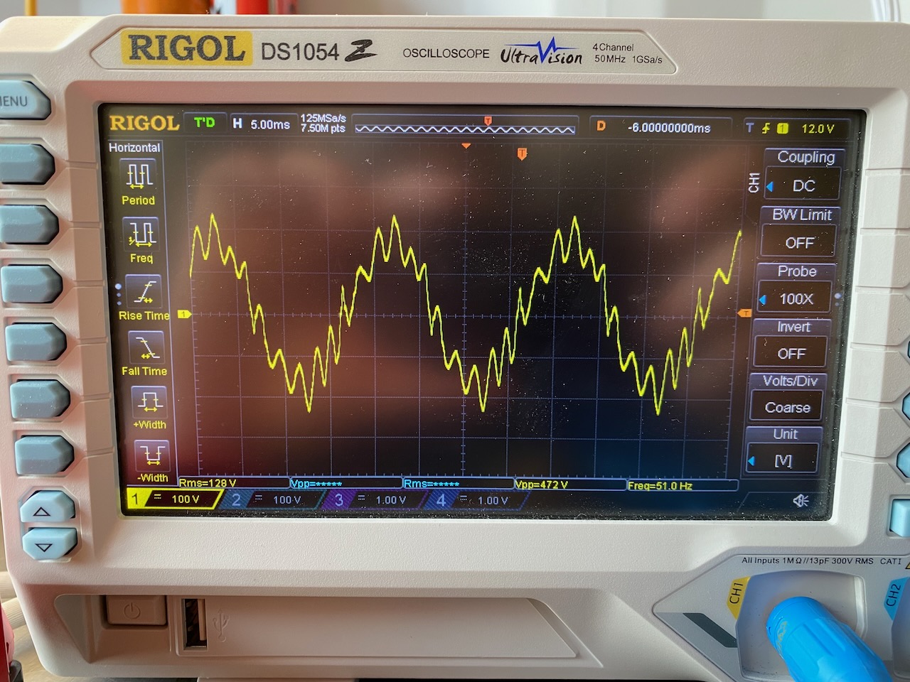
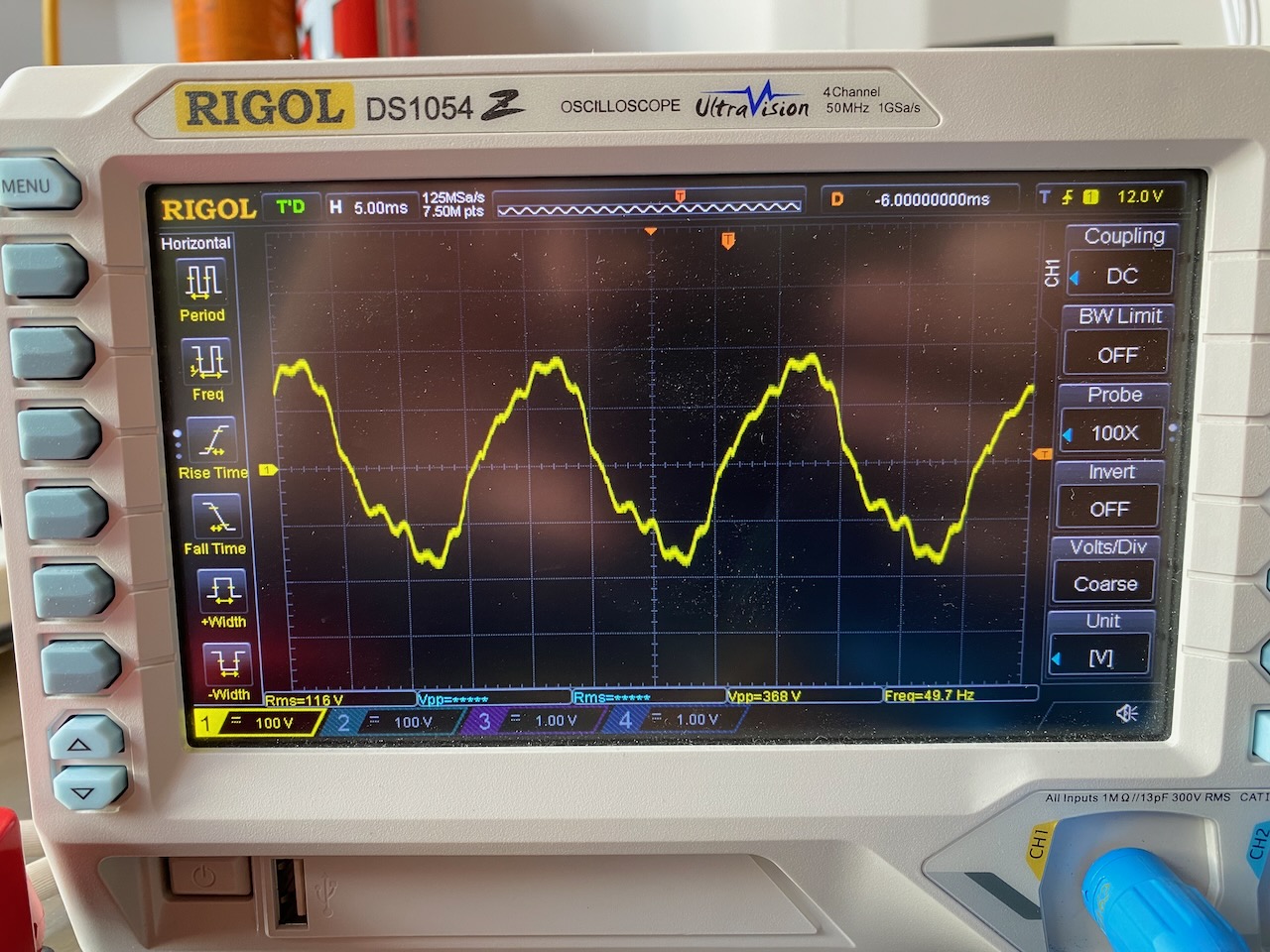
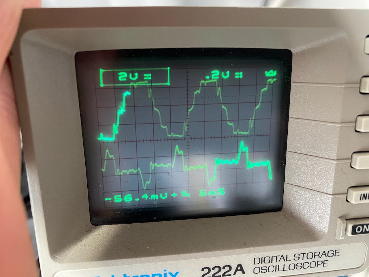
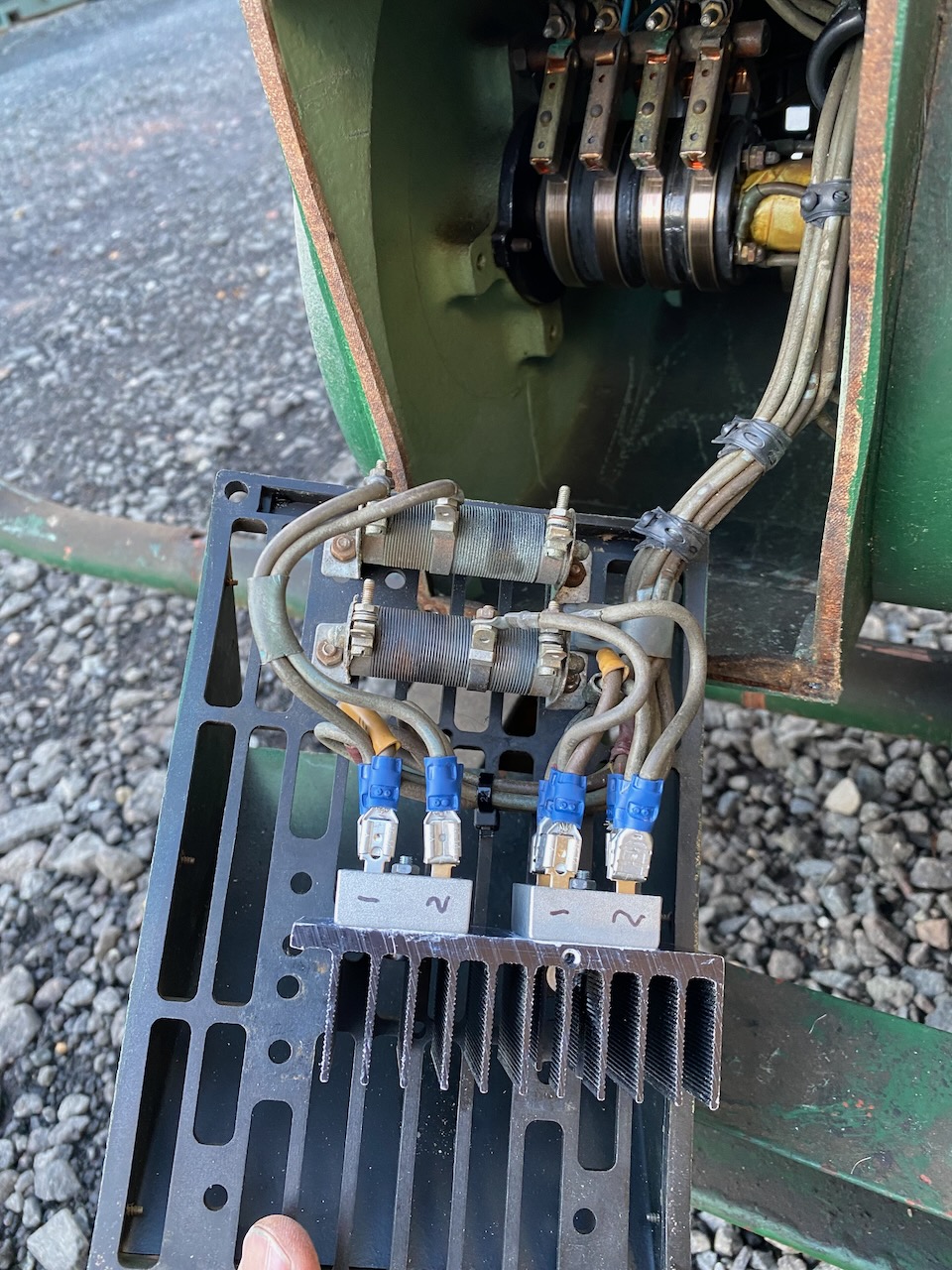
The most important part (as determined by trial and error) is a 2.1kVA autotransformer that steps down 230V to 190. I believe this was originally used to reduce the voltage to street lighting in the early hours as an energy saving measure.
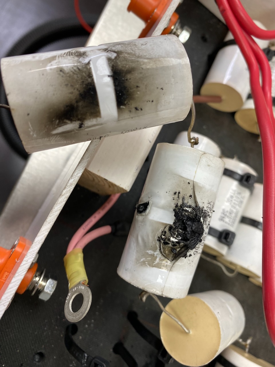
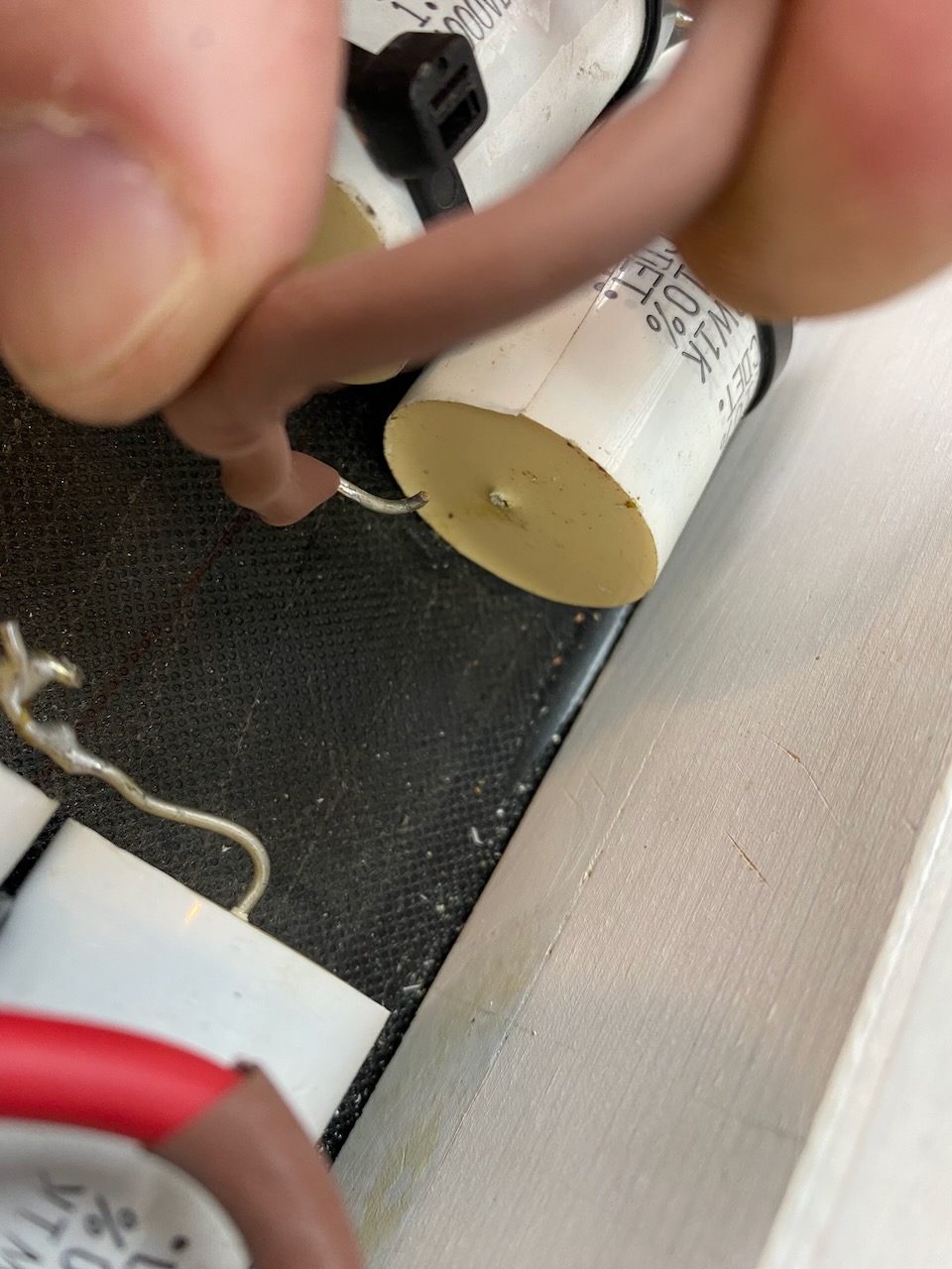
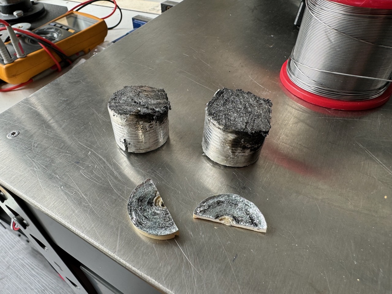
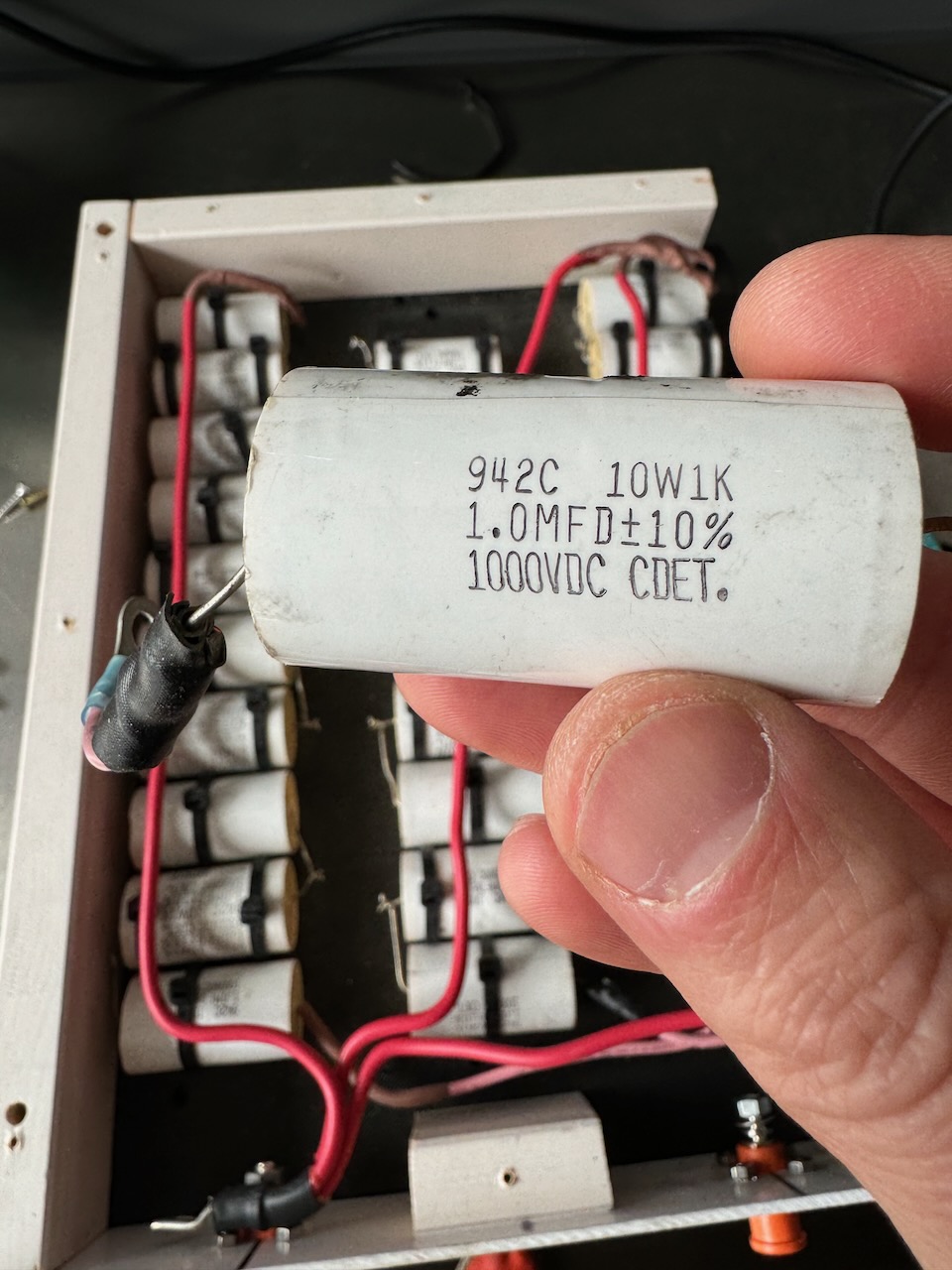
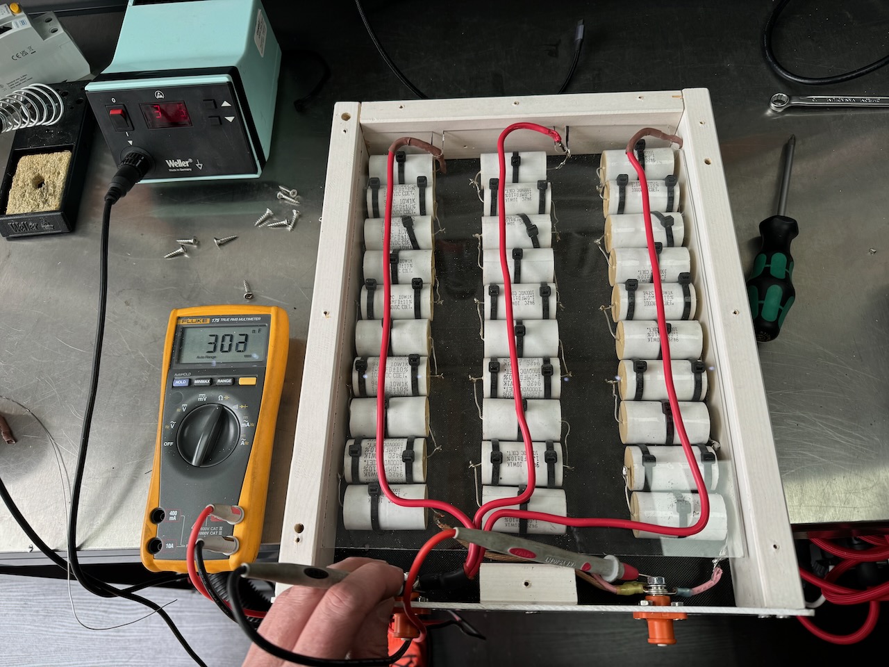
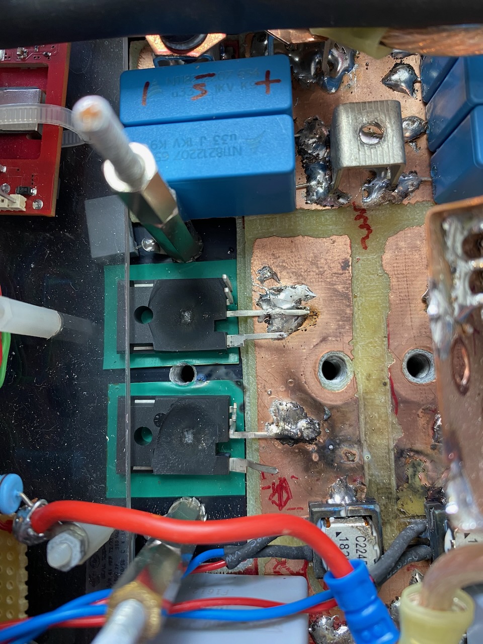
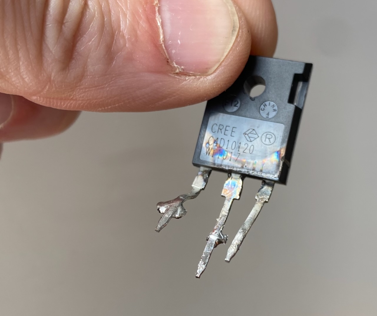
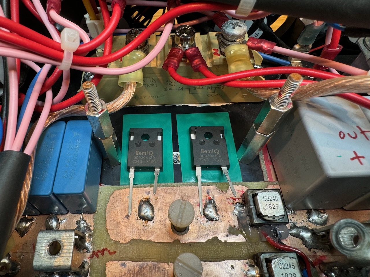
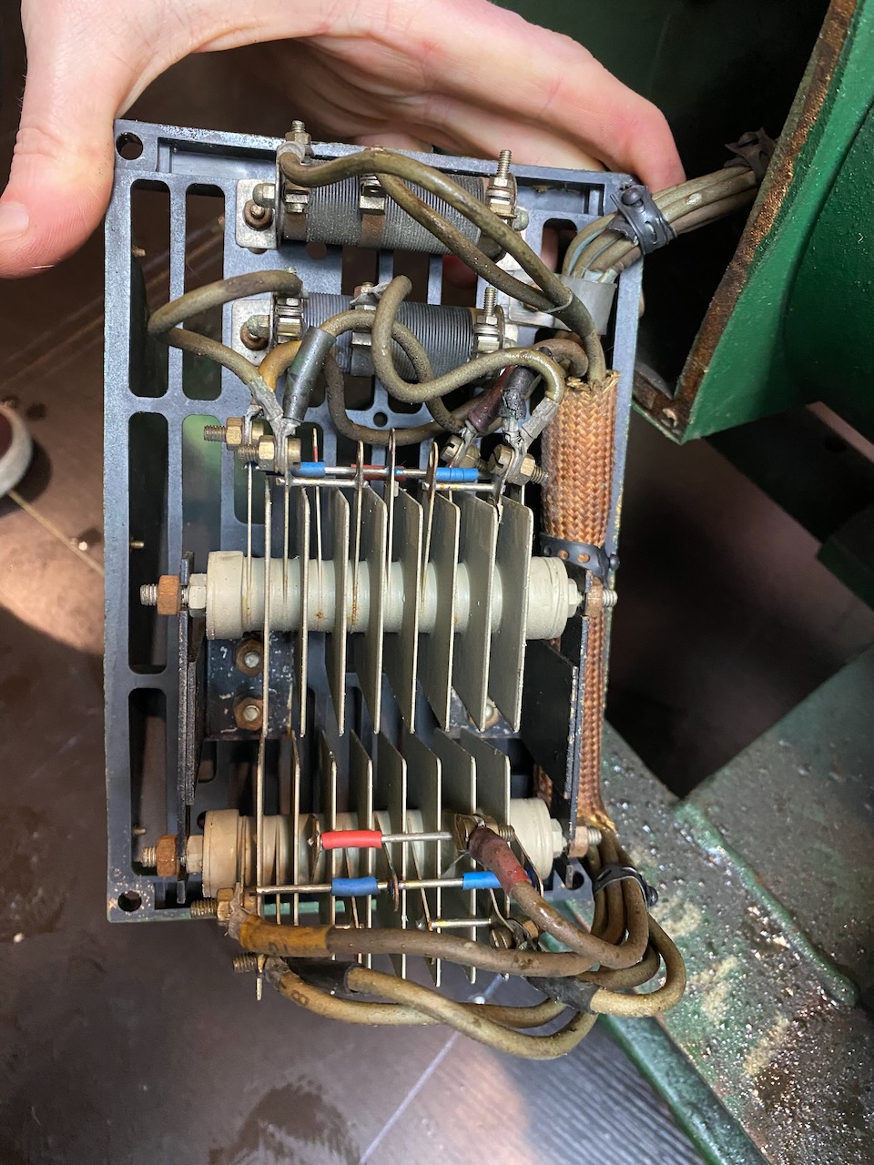
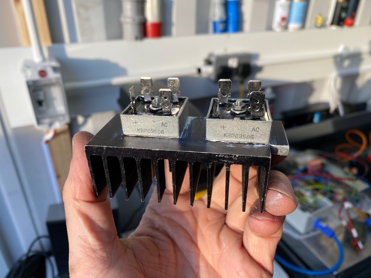
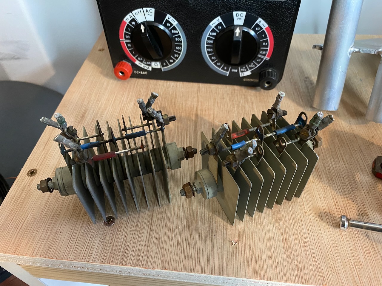
The box also contains a bridge rectifier, capacitor and power resistor (sold as a 230V, 100W cabinet heater) the purpose of which is to draw lots of current on the voltage peaks and squash them down a bit further. This was the final bodge that allowed me to max out the generator’s engine power without any overvoltage trips. Hopefully it should also protect the 12V power supply inside the 3000S from destruction by excessive peak voltage.
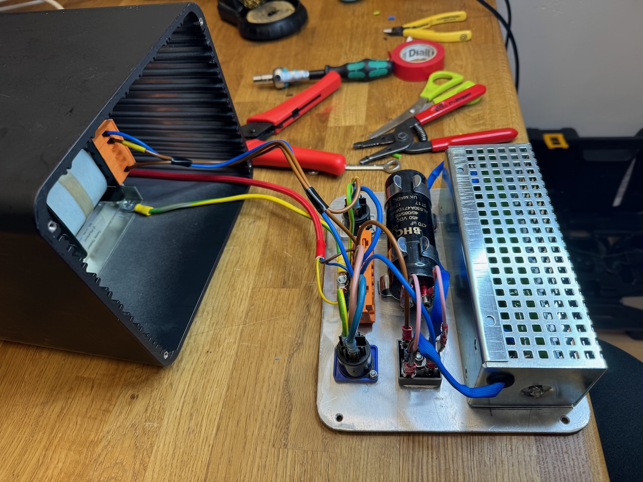
A small fan on the rear panel blows air over the transformer, before it exits through the resistor. This is really a must as the resistor is dissipating about twice its rated power.
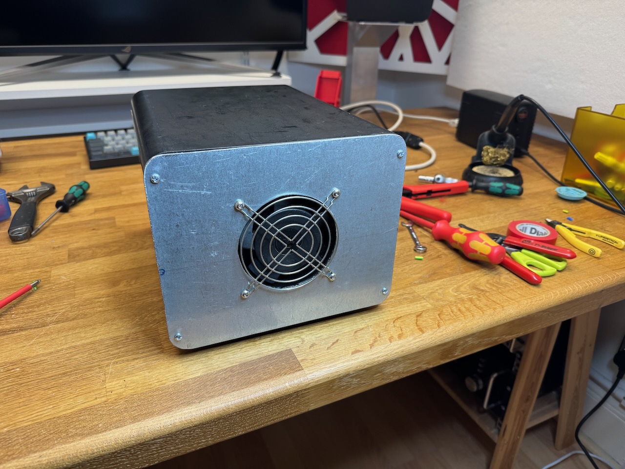
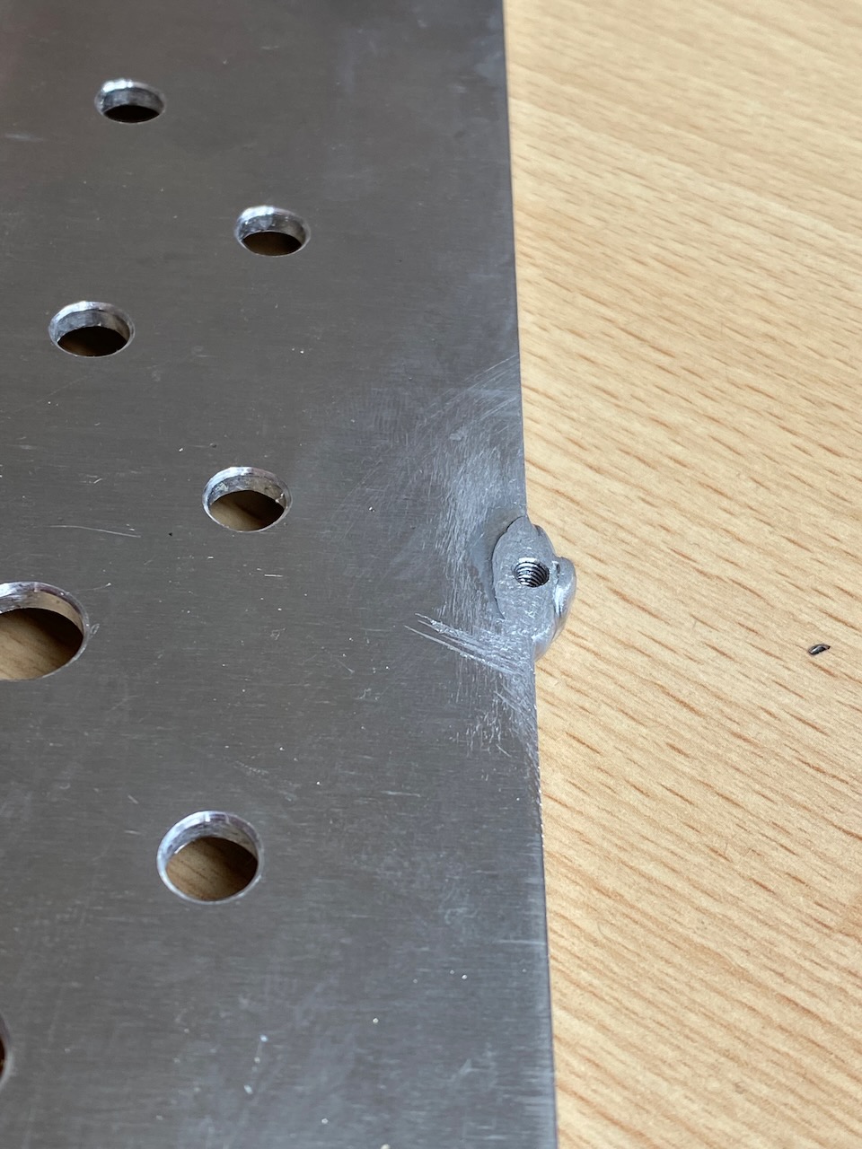
The fan was also salvaged. I can’t remember what it came out of. I had a fun afternoon making front and rear panels out of pieces of scrap metal.
The first of hopefully many happy welds. (proof that a weld doesn’t need to be Insta worthy to be happy 😀 )


