Regular readers will know that I’m a fan of Douglas Self’s Blameless philosophy of audio power amp design. (An uncontroversial choice, as the Blameless topology is not really that different to designs you would have seen in Wireless World in the 1970s, or indeed the innards of Bob Widlar’s opamps.)
Probably the biggest problem I have with the Blameless is the huge bias and offset currents at the inputs, which require a low resistance feedback network to avoid a huge DC offset at the output. This sets off a chain of design compromises and ultimately the carbuncle of C1 and D9 (Fig.1) pops up.
In my previous experiments I tried a matched pair for the input stage, but it made absolutely no difference. The collector currents aren’t necessarily matched, so neither will be the base currents. The biggest improvement was had by using high beta input transistors such as the now-obsolete BC213C. (MMBT5087 would be a suitable 21st century replacement.)
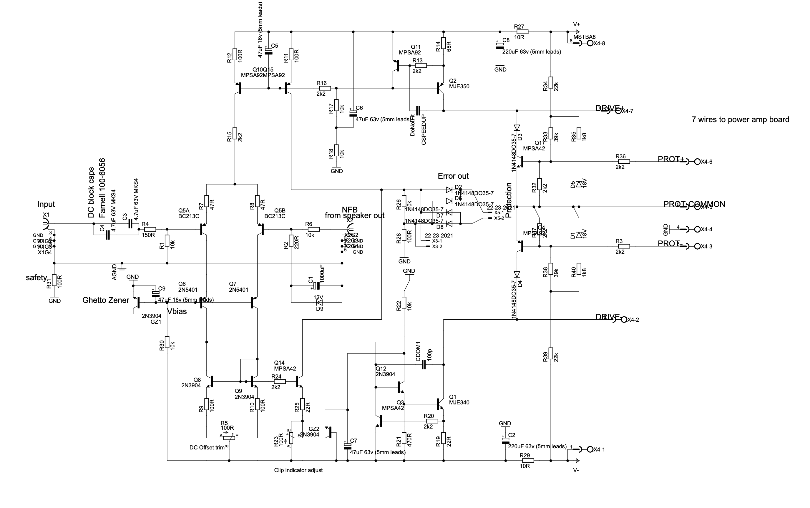
Revisiting this, I discovered that my first attempt at building it was badly unbalanced because of the clip detector (Q14 in fig 1) which robs a lot of base current from Q9. The other side of the mirror has Q12 robbing from it, but Q14 takes much more as it’s a high voltage part with low beta.

By adding a beta helper transistor to the input mirror (Q14 in fig 2) the imbalance due to base currents can be eliminated. The beta helper’s base current is drawn from one side of the mirror, and the base current of the Darlington VAS (Q2, Q17) comes from the other side. By setting R15=R7, Q2 and Q14 will run at the same collector current, so if they are matched for beta, their base currents will also be the same, and the whole input stage will be perfectly balanced to a first order.
(It’s not balanced to a second order because the current drawn from Q14 emitter by Q8-Q11 bases isn’t necessarily the same as that drawn from Q2 by Q17 base, but the imbalance due to this should be tiny. The clip detector can now be hung off Q8, Q9 bases with impunity. 2 transistors are now used to get a 2:1 ratio as required for balance with the current sourced by Q3. I used the same type of transistors as Q8, Q9 for improved balance, so a cascode Q23 is now needed because of their limited voltage rating.)
The other side of the problem was limited beta in the input stage. One of the pillars of the Blameless philosophy is to run the input stage at a high current to give it lots of gm, which you then throw away with emitter resistors. The goal is good slew rate, and the price paid is the high input bias currents.
We attacked the input offset current issue by improving balance of the collector currents (and hence base currents) but if we could reduce the input bias current too, the offset current would decrease still further in proportion.
A promising approach seemed to be replacing the input transistors for Sziklai pairs. (Q6, Q15, and Q7, Q16 in Fig 2.) Now the actual input transistor Q6 can run at a low current (300uA in this case) while Q15 conducts the remainder of the high current needed for decent slew rate. We have a double win because the Sziklai pair is more linear than a plain transistor.
Adding more and more transistors inside a feedback loop is always dodgy, and running one of them at low current where its Ft will be reduced especially so. In this case though, I think the bandwidth will still be adequate. The whole mess is cascoded by Q12, Q13, so there will be no Miller effect to slow Q6, Q7 down. The degeneration from R5, R6 should also help to stabilise things.
The LTSpice simulation of this showed an overall DC offset of 20uV, a huge improvement on my previous Blameless driver board. Of course this is with perfectly matched virtual transistors, but I think the real thing will do pretty well when built with BCM846/856 matched pairs. They specify Vbe to be matched within 1mV, and (what really matters for this circuit) beta to be matched within 10%, which works out at a 100nA worst case input offset current.
The overall result is that the DC offset and clip indicator trims from my original design can be done away with, and the impedances in the input and feedback networks can be increased by a factor of 10, for the same worst case DC offset of about 10mV at the speaker terminals. This means that C1 the obnoxious 1000uF electrolytic can be replaced by something more audiophile grade: the same 10uF plastic film capacitor that used to be the input DC block.
This is what the simulation says, so now I have to build one and see if it works in real life… 🙂
Leave a Reply