A new input stage for the Blameless?

Regular readers will know that I’m a fan of Douglas Self’s Blameless philosophy of audio power amp design. (An uncontroversial choice, as the Blameless topology is not really that different to designs you would have seen in Wireless World in the 1970s, or indeed the innards of Bob Widlar’s opamps.)

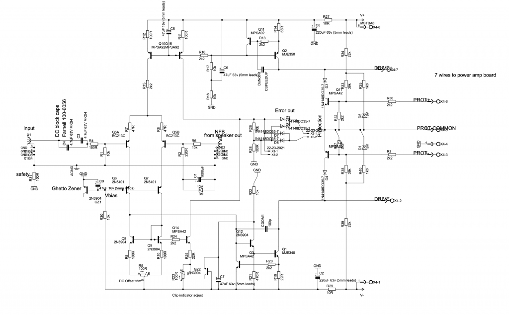
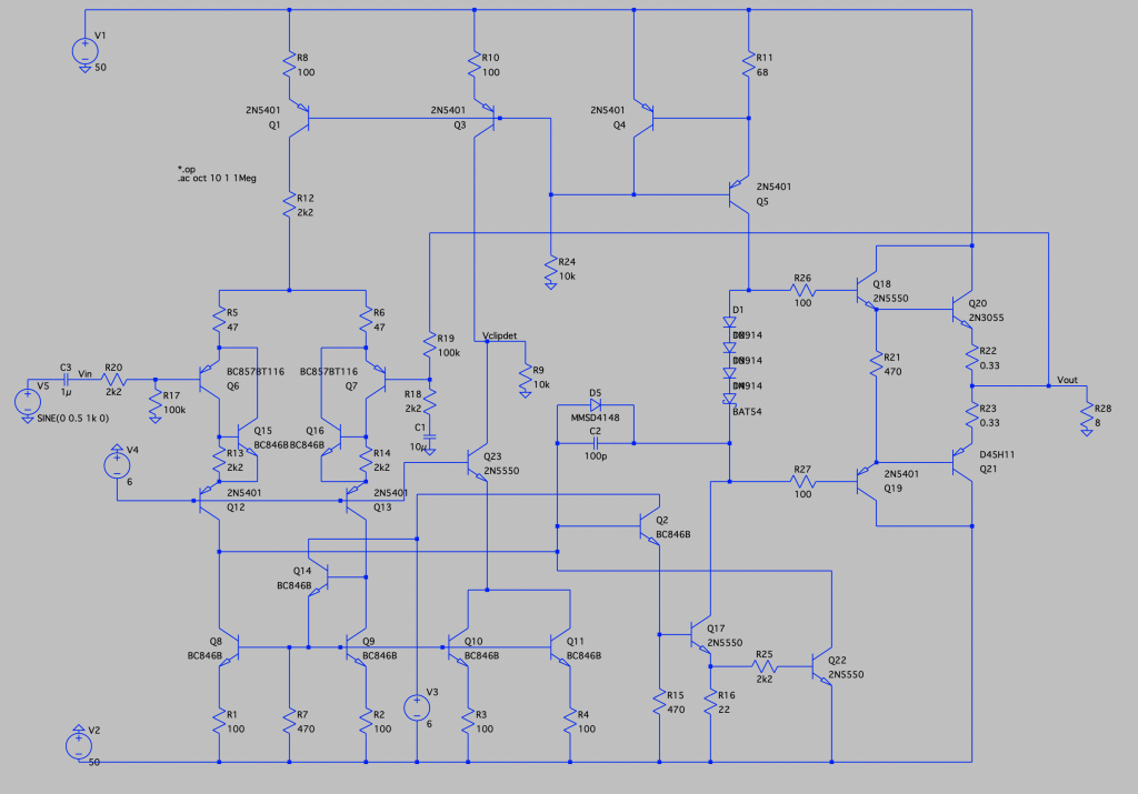
Probably the biggest problem I have with the Blameless is the huge bias and offset currents at the inputs, which require a low resistance feedback network to avoid a huge DC offset at the output. This sets off a chain of design compromises and ultimately the carbuncle of C1 and D9 (Fig.1) pops up.

In my previous experiments I tried a matched pair for the input stage, but it made absolutely no difference. The collector currents aren’t necessarily matched, so neither will be the base currents. The biggest improvement was had by using high beta input transistors such as the now-obsolete BC213C. (MMBT5087 would be a suitable 21st century replacement.)

Fig.1: My original Blameless driver board

Revisiting this, I discovered that my first attempt at building it was badly unbalanced because of the clip detector (Q14 in fig 1) which robs a lot of base current from Q9. The other side of the mirror has Q12 robbing from it, but Q14 takes much more as it’s a high voltage part with low beta.

Fig.2: Improved version (complete model amp in LTSpice)

By adding a beta helper transistor to the input mirror (Q14 in fig 2) the imbalance due to base currents can be eliminated. The beta helper’s base current is drawn from one side of the mirror, and the base current of the Darlington VAS (Q2, Q17) comes from the other side. By setting R15=R7, Q2 and Q14 will run at the same collector current, so if they are matched for beta, their base currents will also be the same, and the whole input stage will be perfectly balanced to a first order.

(It’s not balanced to a second order because the current drawn from Q14 emitter by Q8-Q11 bases isn’t necessarily the same as that drawn from Q2 by Q17 base, but the imbalance due to this should be tiny. The clip detector can now be hung off Q8, Q9 bases with impunity. 2 transistors are now used to get a 2:1 ratio as required for balance with the current sourced by Q3. I used the same type of transistors as Q8, Q9 for improved balance, so a cascode Q23 is now needed because of their limited voltage rating.)

The other side of the problem was limited beta in the input stage. One of the pillars of the Blameless philosophy is to run the input stage at a high current to give it lots of gm, which you then throw away with emitter resistors. The goal is good slew rate, and the price paid is the high input bias currents.

We attacked the input offset current issue by improving balance of the collector currents (and hence base currents) but if we could reduce the input bias current too, the offset current would decrease still further in proportion.

A promising approach seemed to be replacing the input transistors for Sziklai pairs. (Q6, Q15, and Q7, Q16 in Fig 2.) Now the actual input transistor Q6 can run at a low current (300uA in this case) while Q15 conducts the remainder of the high current needed for decent slew rate. We have a double win because the Sziklai pair is more linear than a plain transistor.

Adding more and more transistors inside a feedback loop is always dodgy, and running one of them at low current where its Ft will be reduced especially so. In this case though, I think the bandwidth will still be adequate. The whole mess is cascoded by Q12, Q13, so there will be no Miller effect to slow Q6, Q7 down. The degeneration from R5, R6 should also help to stabilise things.

The LTSpice simulation of this showed an overall DC offset of 20uV, a huge improvement on my previous Blameless driver board. Of course this is with perfectly matched virtual transistors, but I think the real thing will do pretty well when built with BCM846/856 matched pairs. They specify Vbe to be matched within 1mV, and (what really matters for this circuit) beta to be matched within 10%, which works out at a 100nA worst case input offset current.

The overall result is that the DC offset and clip indicator trims from my original design can be done away with, and the impedances in the input and feedback networks can be increased by a factor of 10, for the same worst case DC offset of about 10mV at the speaker terminals. This means that C1 the obnoxious 1000uF electrolytic can be replaced by something more audiophile grade: the same 10uF plastic film capacitor that used to be the input DC block.

This is what the simulation says, so now I have to build one and see if it works in real life… 🙂

Blameless finished!

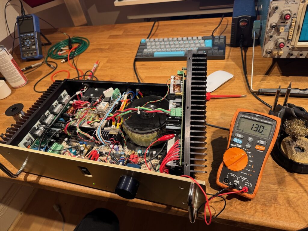
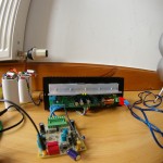
Here it is, pretty much done! The weather was pretty bad this weekend, so I spent most of it in the workshop, wiring everything up.

Besides the stuff I’ve already written about, there is a soft-start module (built rather messily on a tagboard), and a preamp/protection PCB. This contains Douglas Self’s anti-thump and DC offset protection circuit, a thermal cutout circuit using the spare diodes in the ThermalTrak power transistors for junction temperature sensing, and a balanced line input stage using the INA137 and NE5532.

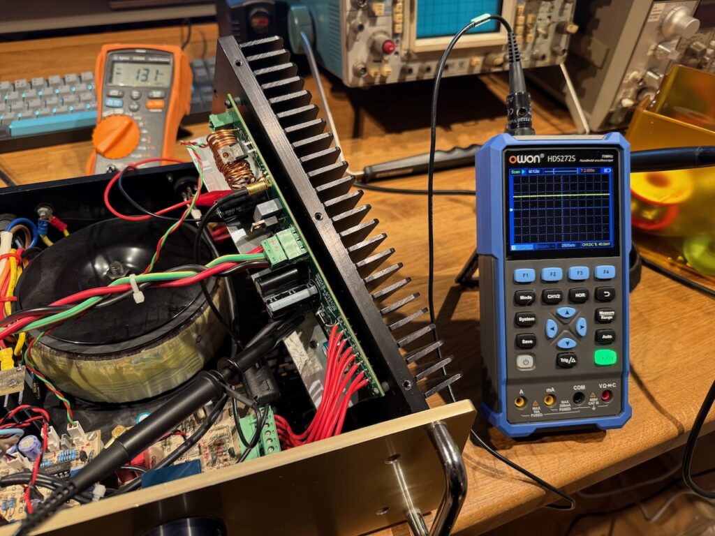
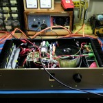
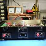
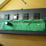
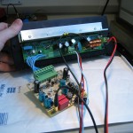
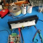
Here are some pics.

Gut Shot 1

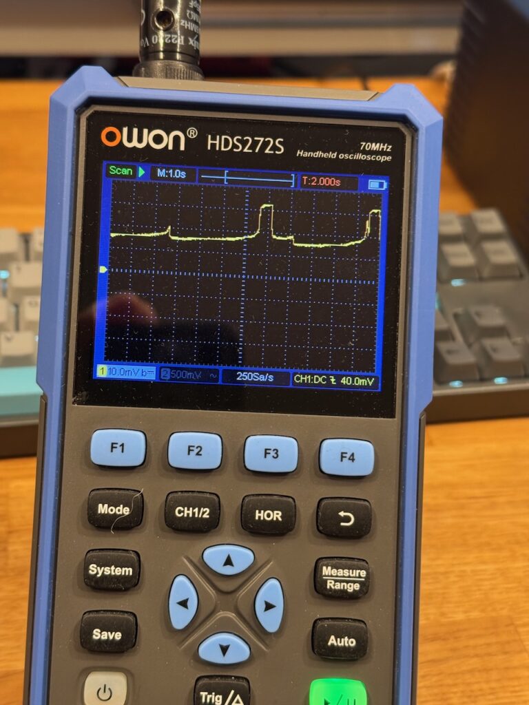
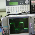
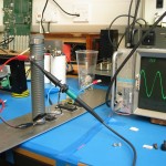
The 10kHz square wave response, just short of clipping, into a dummy load.

I’ll do some whole-system THD measurements some other time. (I broke the Williams Memorial Oscillator. 🙂 )

Power up, distortion down

I did some more work on my Blameless amp project. First of all, I built another output stage, so I now have two output stages, but still only one driver board. Then, I improved my distortion measuring setup a bit. I shielded all the cables and rejigged the grounding, which reduced the oscillator + analyser floor to 0.0036%, with the 80kHz filter engaged.

With this extra resolution I was able to do some more tweaking of the Blameless. I found the following issues:

The MJE350 transistor in the output stage pre-driver is much slower than its MJE340 “complement”. I replaced it with a MJE15033. This allowed me to reduce the anti-sproggie resistor on the base. I was running 100 ohms on the NPN side and 200 on the PNP side, so I changed both to 150 and retried the reactive load test. There were no parasitics, and hopefully I’ll get a bit more power before clipping now.

I was only running about half of the amount of feedback that Douglas Self used in his experiments. (I used the same input stage gm and compensation capacitor as he did, giving the same open-loop gain at 20kHz, but I designed for twice the closed loop gain.) To fix this, I reduced the input pair’s emitter resistors from 100 ohms to 51.

The input doesn’t like being driven straight off the wiper of a 20k volume pot: when I buffered it with a NE5532 op-amp, the noise and distortion went down. I think Douglas Self implicitly designed all his circuits to run best with a 50 ohm source impedance, because that’s what an Audio Precision test set has. 🙂 He runs the input transistors at 2mA for high slew rate and lots of gm, but the downside is lots of noise current and a low AC input impedance. So, in the finished unit I’ll buffer the volume pot.

Adding a DC offset trim and tweaking it for minimum offset also reduced 2nd harmonic at high frequencies. Again this is what Self’s theory of the input stage predicts.

The biggest improvement came by swapping out the expensive PNP matched input pair for a pair of ordinary transistors that just had high beta: BC213C’s with 350 min. as opposed to the 100 typ. of the MAT03. Saving money while boosting performance, that’s more like engineering than hi-fi 🙂

When I was finished with all this, I had a THD+N figure at 100W, 1kHz, 4.7 ohm load, of… 0.0036%! The same as the oscillator itself. The residual also looked identical to the oscillator’s own. At 100W, 10kHz, I got 0.008%, and this decreased to 0.0065% at 100W, 20kHz. (Because of the 80kHz filter, I assume.)

The 1W figures were slightly higher than the above, but from examining the residual, the extra seemed to be mostly the noise floor of the amp and oscillator, rather than crossover distortion.

These are pretty much the best results I’ve had, and I can almost imagine that if I had an Audio Precision, I’d be seeing the kinds of figures that Self claims.

Blameless first sound! :D

Today, after much testing with various dummy loads, including the dreaded 4 ohm reactive one (which showed up some parasitics that I managed to get rid of) the Blameless was finally plugged into a speaker.

It werks!
It werks!

Attempts to measure the THD have so far failed. They really just show up the limits of my  THD measuring system, which is currently no good for anything except finding gross faults.

For instance, the reading I previously got of 0.05% at 10kHz and 120W. When I took the amp out of circuit and connected the analyser straight to the oscillator, the THD reading increased to 0.09%.

The THD analyser does show up crossover spikes, though, if the output stage is underbiased. They were pretty much invisible by a bias voltage of 10mV per side (20mV total) which corresponded to 200mA total idle current. I set it to 13, which gives the 26mV total that some experts recommend.

Anyway, it’s working, and experimenter expectancy notwithstanding, not to mention lack of one channel, I swear it sounds better than my old MOSFET amp. Maybe there is something in Douglas Self’s claims of poor crossover distortion from MOSFETs. Once I get the other channel built and the system put together, I will make that low-distortion oscillator and do a THD shootout. Or an ABX test or something. Anyone want to lend me an Audio Precision test set? 🙂

More Blameless progress

The Blameless project is grinding on!

.

4-layer boards for the output stages were designed in Eagle and ordered from PCB Train. Some samples of the ONSemi NJL4281/4302 transistors with built-in thermal sensing diodes were obtained. The whole lot was fitted to a large heatsink using Sil-Pad A1500 high performance thermal pad stuff.

After testing using a bench power supply, it was connected to a large transformer, rectifier and some capacitors.

The power was turned on and amazingly it failed to explode.

More detailed info to come, but the maximum output is about 120-150W into 4 ohms, the THD about 0.05% or less at 10kHz and 120W (so should be nearer 0.005% at 1kHz) and the short circuit protection, thermal compensation etc. all works as planned.

First THD analyser results!

I’ve finally got the THD analyser hooked up and working! Not very well, though, because I have to use it with my not-too-hi-fi signal generator, on account of the analyser’s own oscillator section being AWOL. My sig gen is DDS-based, so it puts out lots of high-frequency crud and DAC quantization errors, and these overwhelm the amp’s own contribution to the residual. Except if I test at 10kHz and press the analyser’s low-pass filter button, which kind of fixes it…

Anyway, I hooked the Blameless up to an unregulated power supply to pump in plenty of hum and grunge (got to test that ripple rejection too!) and made some THD + Noise measurements.

THD test setupTHD at 50W50W residual

10kHz, 50W into 4 ohms: 0.086%

10kHz, 2W into 4 ohms: 0.037%

(I measured at 10kHz to try and force the amp to generate more noticeable THD levels. And yes I have the hi-pass button pressed: some hum is getting in somewhere…)

I also tried setting the bias pot to minimise THD.  At 50W, this happened at a setting so cold that there was barely any bias at all! I measured a Vq of around 300uV. But at 2W, the minimum occurred at a Vq (across each emitter resistor) of about 14mV.

2W THD, underbiased2W THD, bias just right2W overbiased

I think what’s happening is that at high power and high frequency, an overly cold bias helps to counteract the transistors’ slow turnoff. Too cold bias effectively starts turning them off in advance. This gives a false THD null. 2W seems to be a better power level for setting it.

At both power levels the THD nulls were very broad, and seemed to stay stable when I let the heatsink get burning hot, and then applied a fan to cool it back down.

Still a long way to go in terms of refining the THD measuring setup… but it’s a start!

Blameless short circuit protection

So, now the short-circuit protection is tested.

I used a dual-slope VI limiter as described by Self in his book, except I simulated it in LTSpice and played with the component values to lower the power dissipation a little. Self’s original design allowed the transistors to dissipate nearly their full rated 250W, and I thought that was excessive, since it’s only possible at a case temperature of 25’C, and that will never happen in practice.

I guess his reasoning is that since the amp will only amplify AC signals, then under short-circuit conditions each transistor will conduct with a duty cycle of 50%, so the mean dissipation will only be 125W. But I can imagine situations where that wouldn’t work.I also plan to try the NJL4281/NJL4302 transistors in the future, and these have less SOA than the MJ15024/MJ15025, the devices that Self designed the circuit for.

My new values were supposed to make the circuit limit at about 125W. Anyway, so I made the circuit up and tested it with the method described on Rod Elliot’s site. Namely, I shorted the amp’s output with a 0.1 ohm resistor, and fed 100us pulses at a repetition rate of 10Hz to the input. I did this with the amp running off two regulated supplies, allowing me to vary the rail voltage and note the current for each voltage.

At first, the negative rail had no limiting at all! It started out at 12A and headed skyward from there. It turned out that I put a diode in backwards, and also the gain of the PNP limiter transistor was low, and the VAS current limit was a little high. Once I got that fixed, I plotted out the two sets of results in Excel, and added loadlines for reactive and resistive loads on 40V rails.

Protection locus

So you can see that with one pair of output transistors installed, we can just barely drive a 4 ohm resistive load or an 8 ohm reactive one. To drive a 4 ohm reactive load, we’d need two pairs, which is what I was expecting, and two pairs is what I plan to fit.

Finally as a sanity check I rigged up a reactive load: A big iron cored choke wound with about 80 turns of heavy wire. I put two 4.7 ohm resistors in series with it, and it could drive that easily at any frequency. Go down to one 4.7 ohm resistor, and I found a frequency where the limiter would activate and cause crazy clipping, like in Rod Elliot’s Figure 4 linked above. Again this agrees with what I expected, so we’re good to continue!

Note that before trying this test, I added the catch diodes from the speaker output back to the rails. Otherwise the output devices would be destroyed when the limiter kicked in.

My Blameless is working!

I’m so happy! Ever since I was a humble EE student, I’ve wanted to design my own hi-fi power amp based on Douglas Self’s “Blameless” philosophy. I now proudly present the prototype.

doesn’t look goodbut seems to work well so far

I’ve built power amps from other people’s designs before, but this is the first one I’ve designed, albeit with a lot of help from Self’s “Power Amplifier Design Handbook.” It’s a modular system, with a driver board that can be hooked up to any kind of output stage, to make different kinds of experimental amps.

It’s still not finished: the protection circuitry and THD need testing. But it’s passed the first hurdle, in that it can run with a good DC offset (I measured 16mV), stand +/-60V rails and drive a load without blowing up.

The last three amps that I’ve built were powered by valves (tubes?), and the two before that had MOSFET output stages, so working purely with BJTs was a bit of a culture shock. Self always argued that they were the best amplifying devices, and they certainly seem pretty good. The OnSemi MJ15024/MJ15025 pair of transistors I used in the prototype cost a few dollars each, less than half the price of equivalent MOSFETs, and they make as much Umph as a pair of KT88s. They didn’t want to oscillate or explode, and the whole thing generally just worked first time. Apart from that evening I slipped with the scope probe and took out half a dozen trannies in the driver board.

This is something of a multicultural project. The output trannies were made by Motorola in Mexico, all of the other ones came from Continental Device in India (that’s what you get when you buy Farnell’s “Multicomp” value brand transistors) and the whole mess was assembled by a Scotsman wired on Fairtrade coffee beans.

And yes, Self convinced me to buy a distortion analyzer. So far all it’s told me is that I need to get a better signal generator.