Guide, please explain the scene. It is tangled colours, jumbled like a dream. A petrol-slick of possibilities Not unlike the sun through screwed-up eyes.
Graffiti leaps out from the walls There’s light and shadow, shape and form The architecture’s come alive Touch the concrete here, it’s warm
It’s evening now, the golden hour Oh quick, you’ve got to shoot! You’ve hardly any eyesight left. The composition’s up to you.
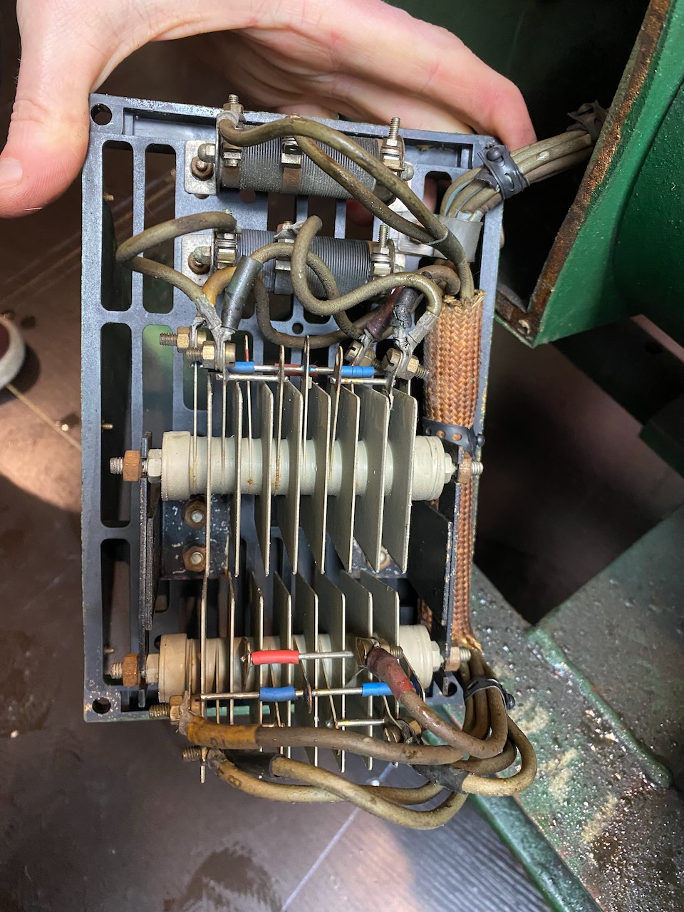
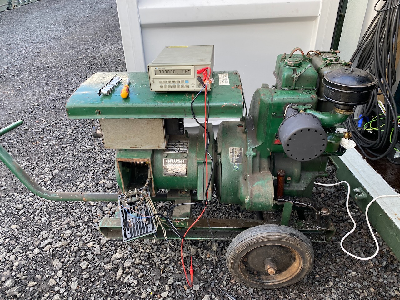
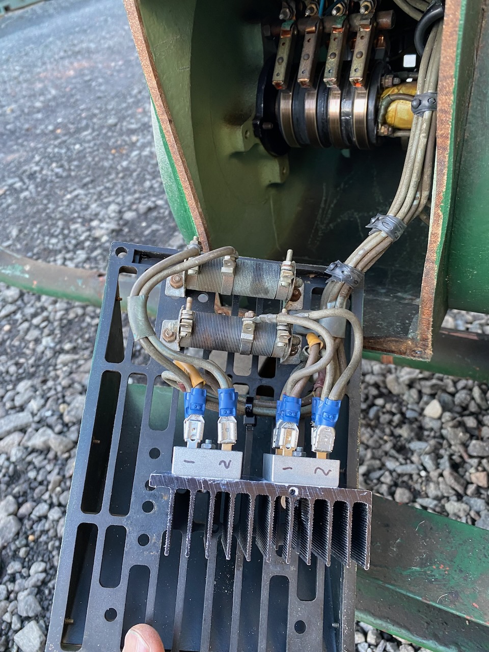
After a period of working OK Lister’s output voltage began to sag horribly under load. The selenium rectifiers are known to be unreliable so I decided to replace them.
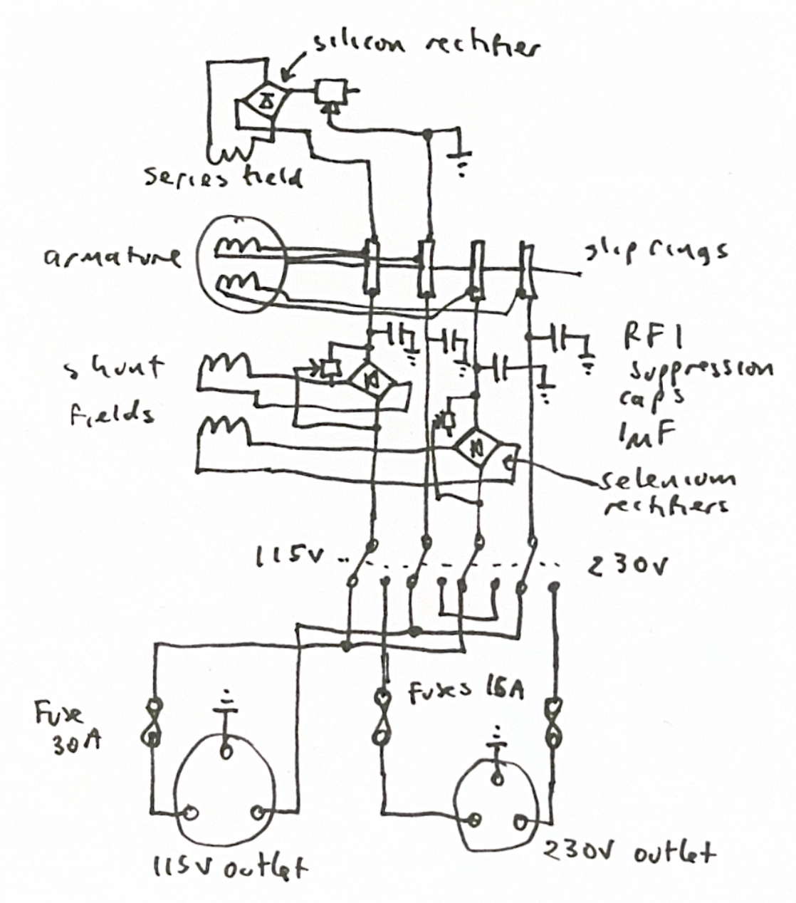
The below schematic shows how the Brush 3kVA alternator is wired (Brush connection diagram 9840322)
OOps, the series and shunt field labels are swapped.
The generator has both shunt and series fields. A silicon bridge rectifier provides excitation for the shunt field while the series fields are energised by a portion of the load current, through the selenium rectifiers. The armature and series fields are in two identical sections that can be switched in parallel for 115V or in series for 230.
Note that in 230V mode the output is centre tapped to earth. Both live and neutral pins of the outlet have 120V on them. This seems to be a design decision by Brush to reduce the risk of electric shock, however it means that live and neutral both need to be fused.
I took the opportunity to do some 4 wire resistance measurements while the wiring was disconnected. One section had a series field resistance of 0.20 ohms and a diverter resistance of 1.00 ohms. The other had a field DCR of 0.21 and the diverter resistor was set to 0.87. This resistor was burnt from a previous short circuit so I cleaned it and reset to 0.96 ohms using the unburnt end.
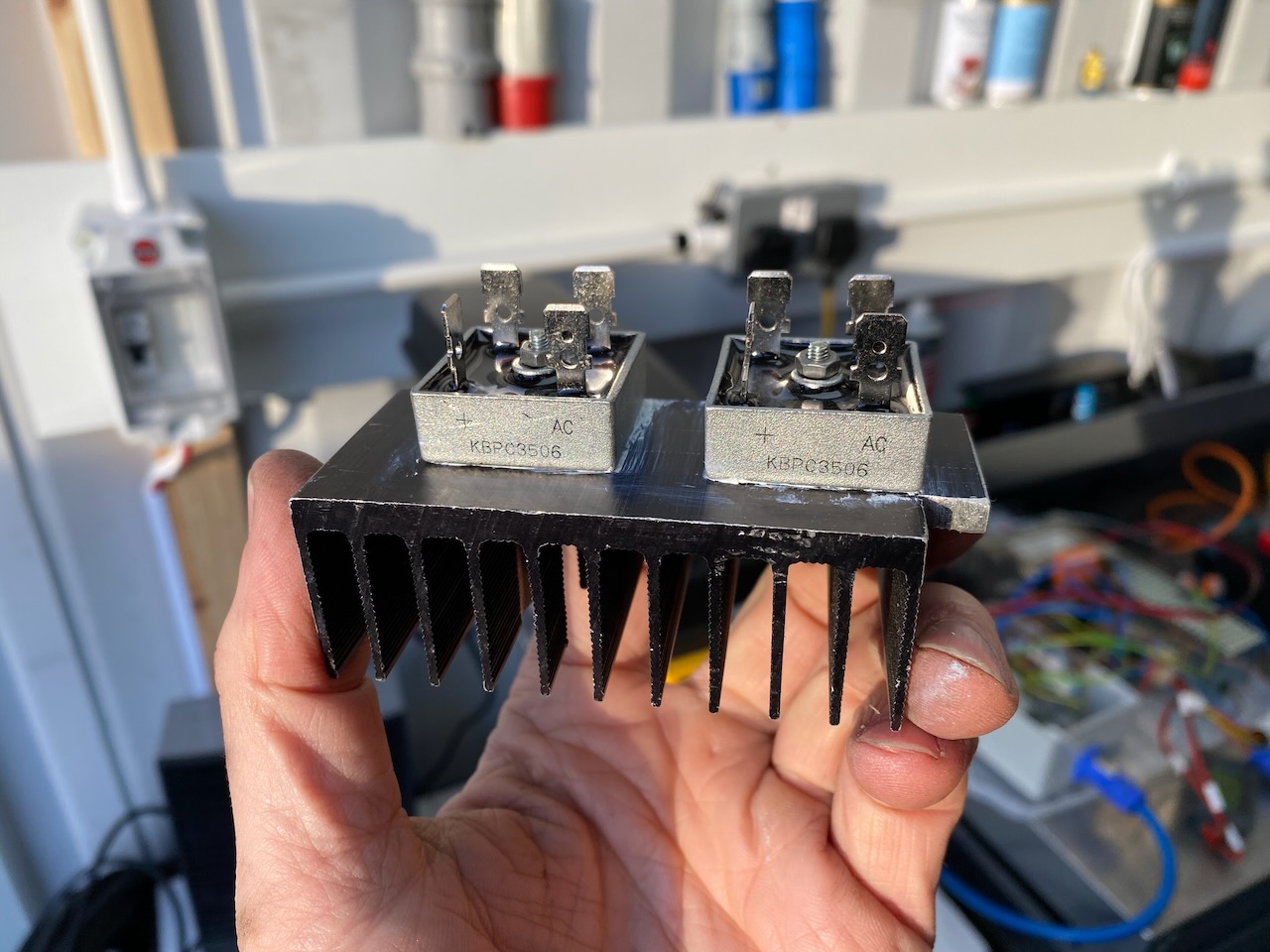
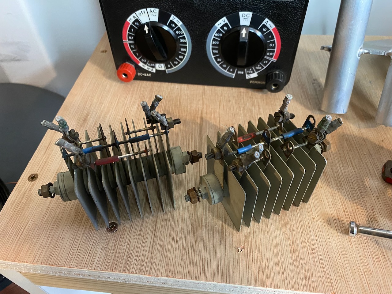
I prepared two KBPC3506 silicon bridge rectifiers on a heatsink. These are an inexpensive 35A 600V part available from many distributors.
The new rectifiers are much smaller so I was able to get rid of a lot of wiring, and that sketchy looking woven tube that was probably asbestos.
Of course I saved the original rectifiers, lol no, they went straight in the toxic waste.
This year’s Gaussfest was mostly remarkable for forgetting the drum machine. :<
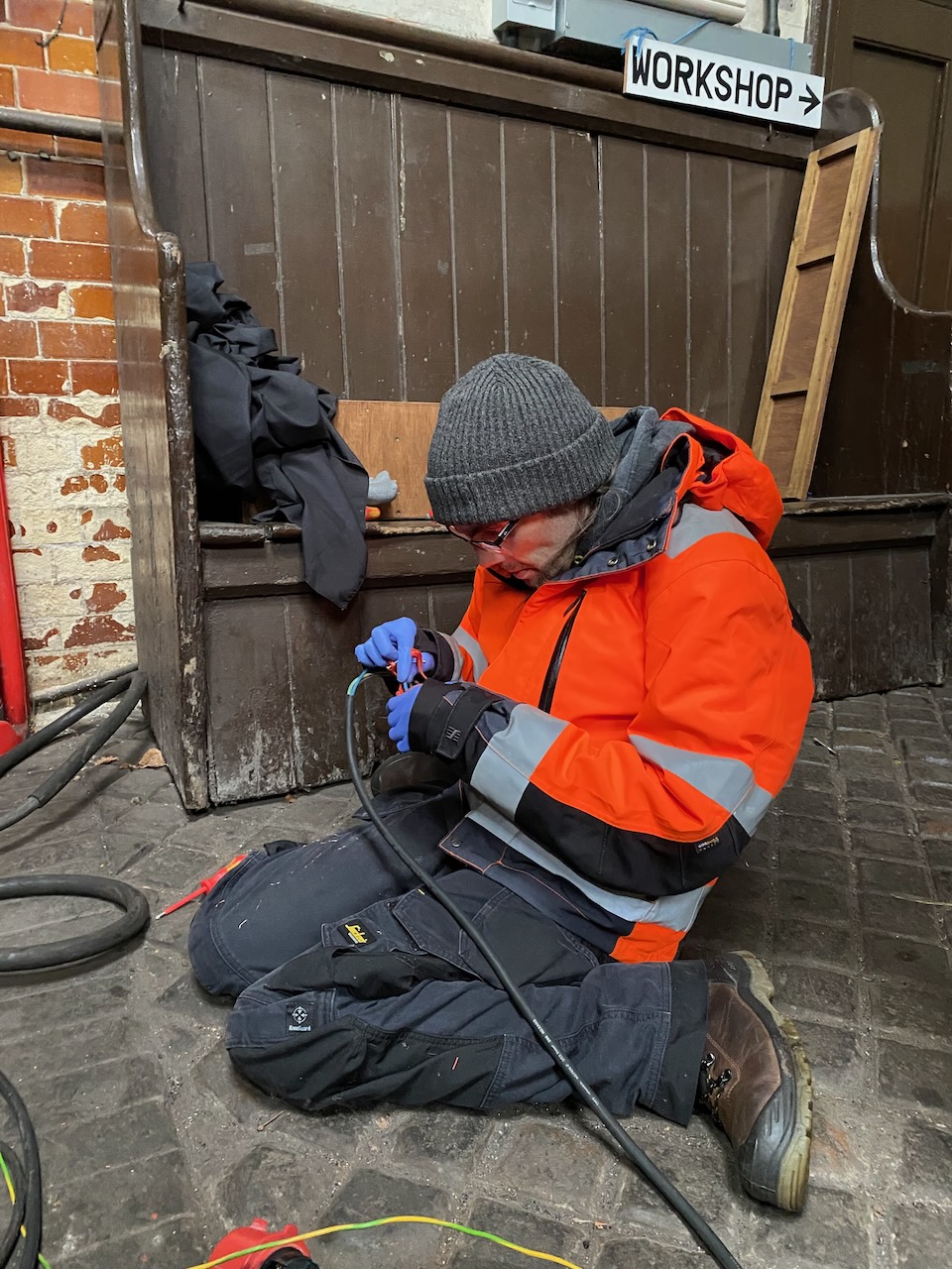
Octavia is so full of stuff… but no drum machine 🙁Papplewick Pumping Station never fails to impressAdam Horden helps wire up the 3 phase power supply while I pester him with questions about public liability insurance.Jeb from Lords of Lightning ready to be zapped by Odin.
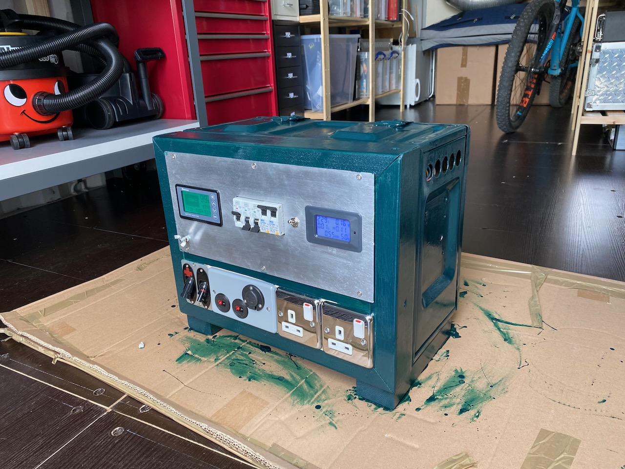
Fittingly the paint colour is Valspar “Thunderbolt” left over from painting the front door at home. Still waiting on some more industrial looking socket outlets to replace the chrome ones.
I’ve been warned that after going to Powerpole connectors for 12V DC distribution, I’ll never want to touch a cigarette lighter plug again. That sounds about right.
Each year the leaves fall a little more, The thickened tree-arms spark With frost in the park, where other middle-aged men Kiss dogs that don’t belong to them.
These men consume their friends like food. But underneath pond-scum and weeds A man retains his hair, his needs. Why won’t you stay for good?
I am planning 3 weekend expeditions with the goal of ending up on Beinn Mheadhoin in the Cairngorms for my 141st Munro. The name means “Middle hill” and 141 is halfway round…
Expedition 1: Wild camping in the Alders *DONE* Munros 126-131 This expedition ended up done the other way around: setting off from Luiblea Saturday lunchtime, bag Geal Charn and Creag Pitridh, go via Bealach Leamhain and An Lairig to bivvy spot at Diollaid A’Chairn on Aonach Beag ridge, then following day bag ridge and return to Luiblea via track at Luibvan. Nav by map and compass in low cloud throughout
Day 1: Geal Charn, Creag Pitridh. Day 2: The Aonach Beag ridge: Carn Dearg, Geal-Charn, Aonach Beag, Beinn Eibhinn
Expedition 2: Up the Fannaichs *DONE* Munros 132-140 Thanks Allan Do 4 one day and 5 the other bringing the Munro count to 140- with support from a friend who did the same thing in February
Expedition 3: The Gorms *DONE* Munros 141 and 142 Bag Beinn Mheadhoin from Glenmore Lodge via Loch Avon, taking in Bynack More on way home.
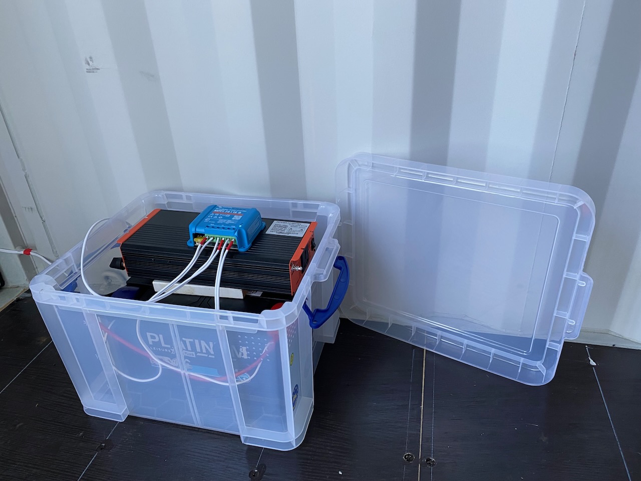
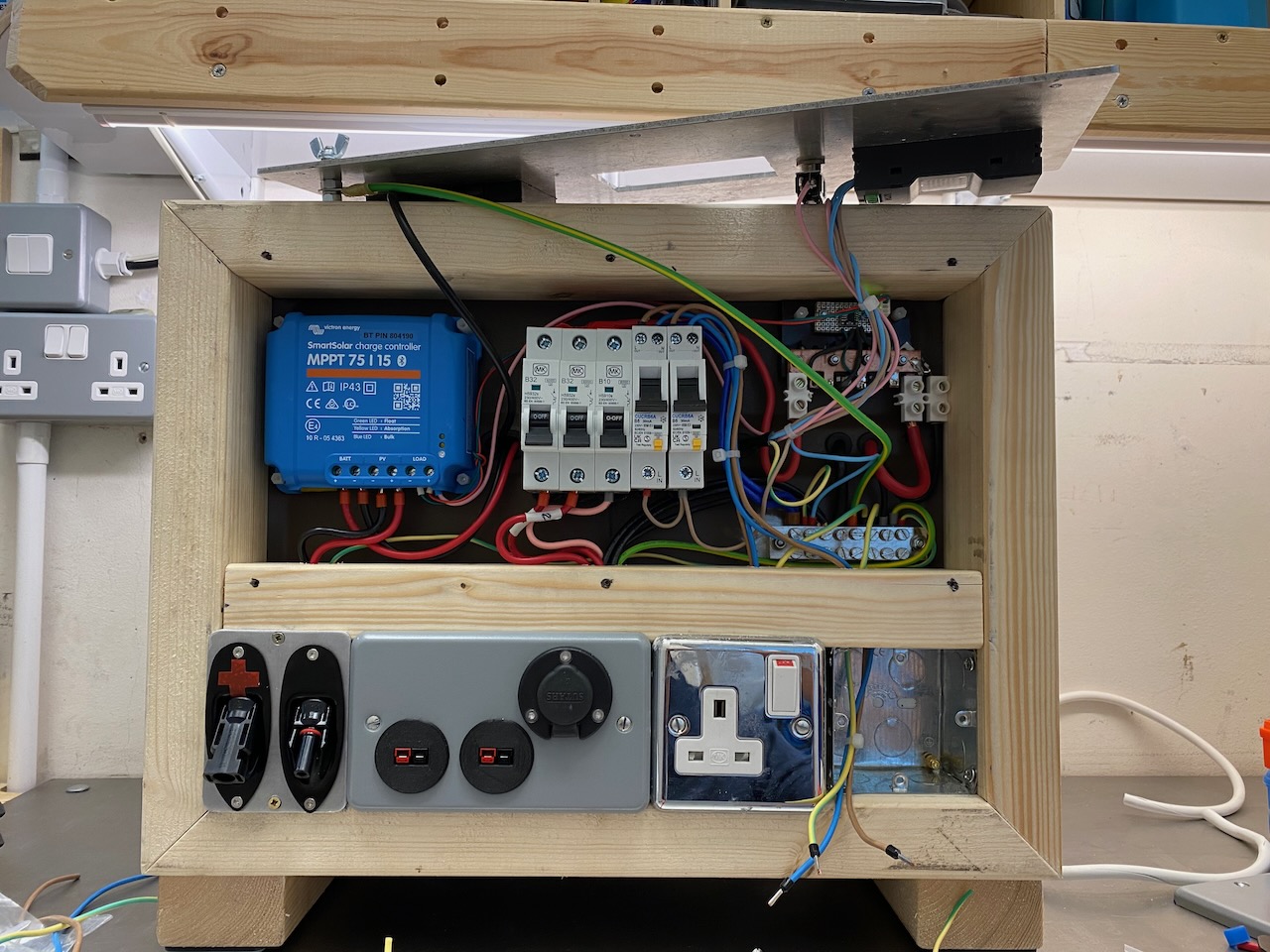
I’ve been renting a 20ft container to use as storage and workshop space, and wanted some electrical power.
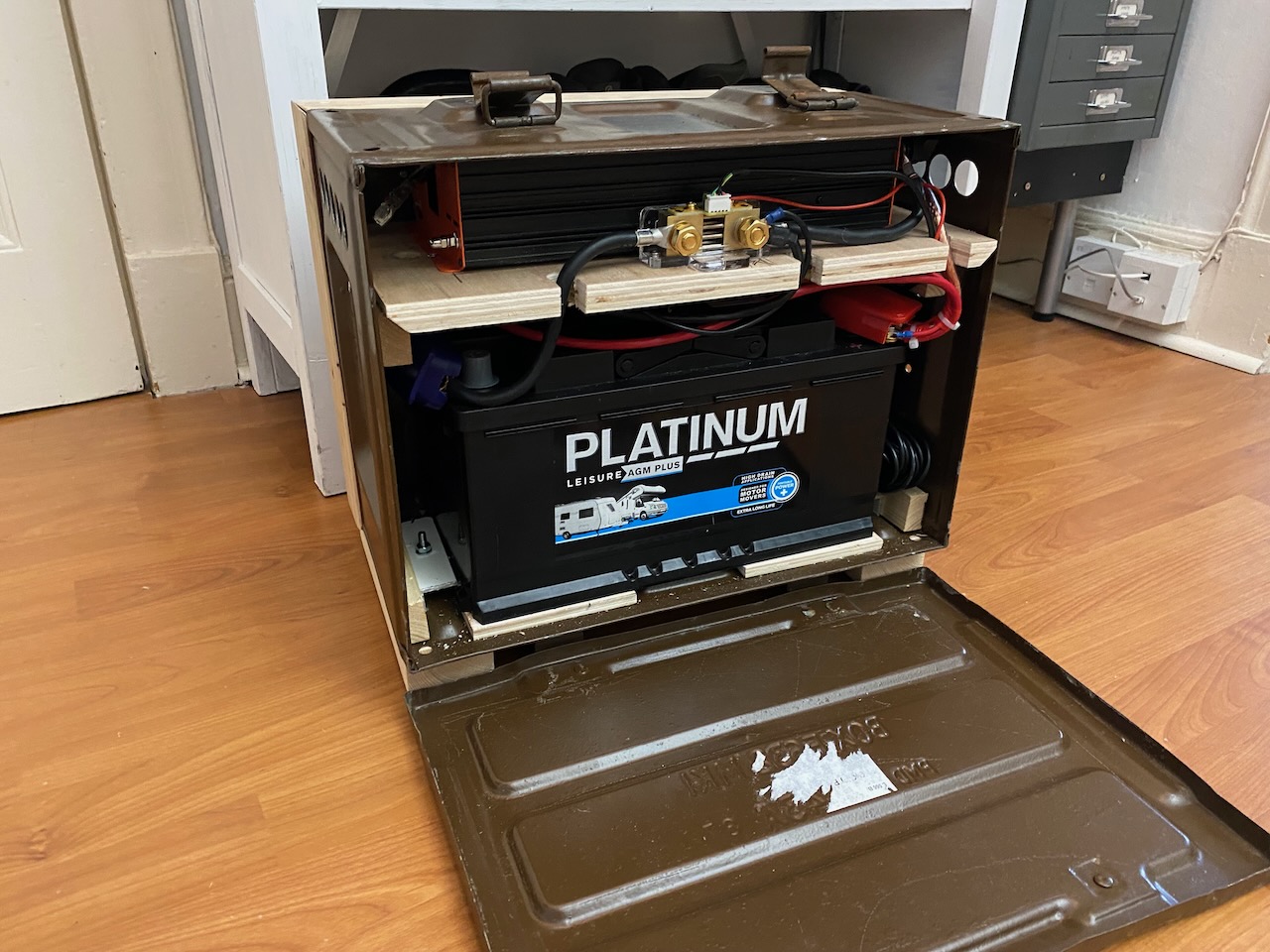
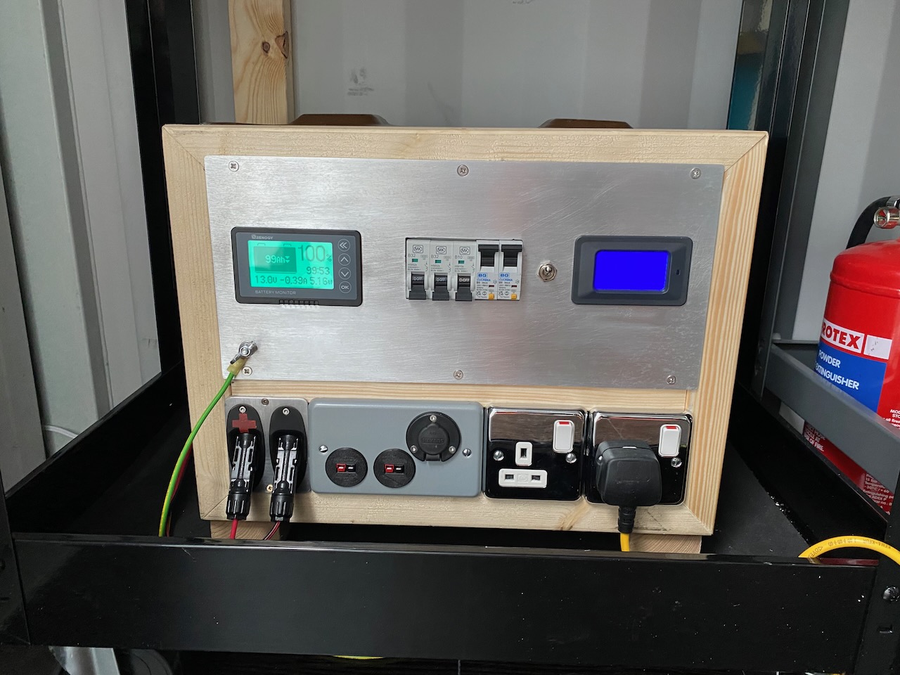
The prototype was not very elegant. 😀 The basic components are a 135W solar panel on the roof, a 12V 100Ah AGM leisure battery, a Victron MPPT charge controller, and a 1kW pure sine wave inverter.
The inverter is a reasonably priced “Mercury” branded unit from TLC Electrical. I believe the Chinese OEM is Ningbo Kosun. I may do a more detailed review in another post.
Lead-acid batteries aren’t great for geek points, but I thought it would be the best technology for the job. I only visit about once or twice per week and rarely drain the battery completely. It can also get very hot in there in summer, so the battery figure of merit I’m interested in is basically calendar life when fully charged at high temperature. Lead-acid offers a lot of that for the money.
The first problem I found is that the Victron’s load output is wimpy. It won’t even run a 12V compressor. However the Victron has a good algorithm for turning off the load when the battery gets low to avoid damaging depth of discharge, and I wanted to make use of that.
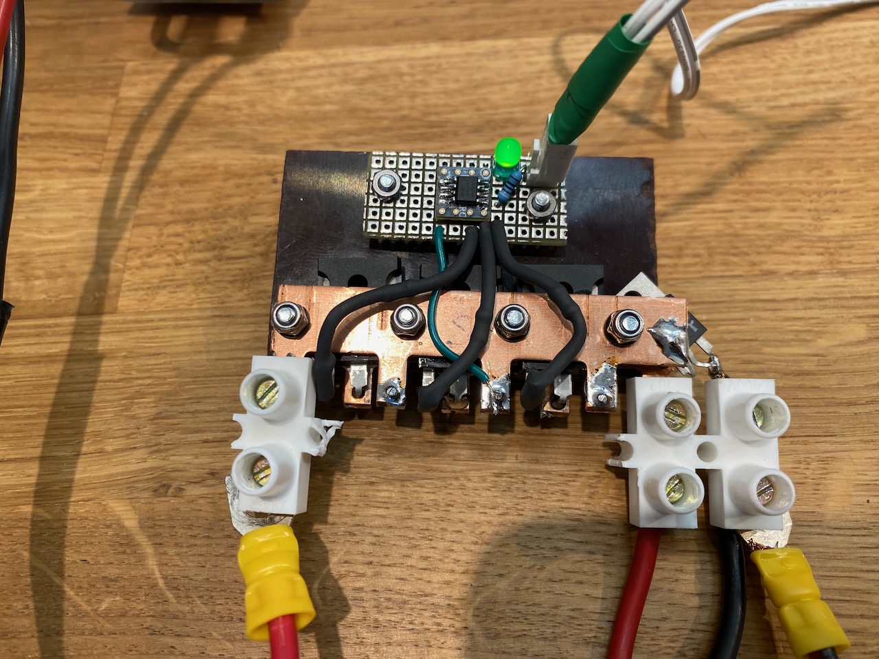
So my first addition was a large MOSFET solid-state relay that would allow the Victron load output to control a much heavier load at 12V. I made this myself using 3x IRFP7430 MOSFETs in parallel, driven by a Si8712 isolated driver chip. The MOSFETs are rated at 40V, 195A, 1mOhm Rds(on). Turn-on and off seems to be rather slow. The small package on the right is a flyback diode to avoid a large transient when turning off an inductive load such as a motor. The MOSFETs would probably be ok with this, but it could damage other loads on the 12V bus.
The solid-state relay does not switch the supply to the inverter. This is connected directly to the battery to minimise voltage drop.
I modified the inverter to have a remote on/off switch, which was very easy as the internal on/off switch just connects 12V from the positive input terminal to the control circuitry. I simply hacked it so the control circuitry got its 12V feed from the Victron’s load output via a front panel toggle switch. This allows the Victron’s low battery algorithm to turn off the inverter alongside the other loads, and allows me to bury the inverter inside the enclosure with no access worries…
Note that I couldn’t find the official remote control panel for the “Mercury” inverter. I bought what I thought was the correct one on eBay, and on plugging it in, there was smoke… Luckily it all came from the remote and the inverter still appeared to be in good shape.
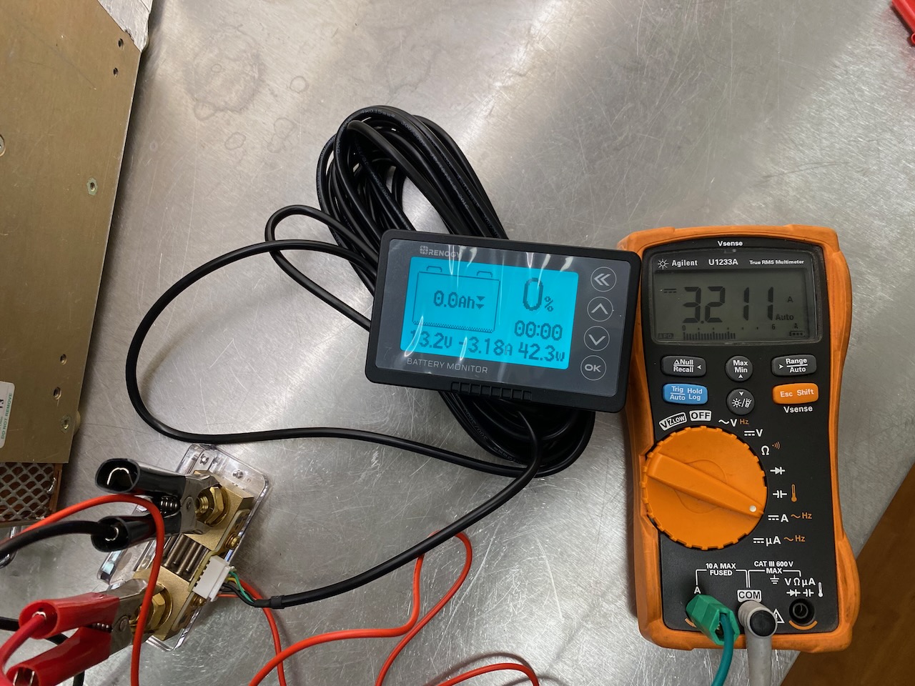
I also got this 500 amp battery monitor in Renogy’s Black Friday sale. 500A is overkill but it was cheaper than the lower current versions. The accuracy at low currents turned out to be fine.
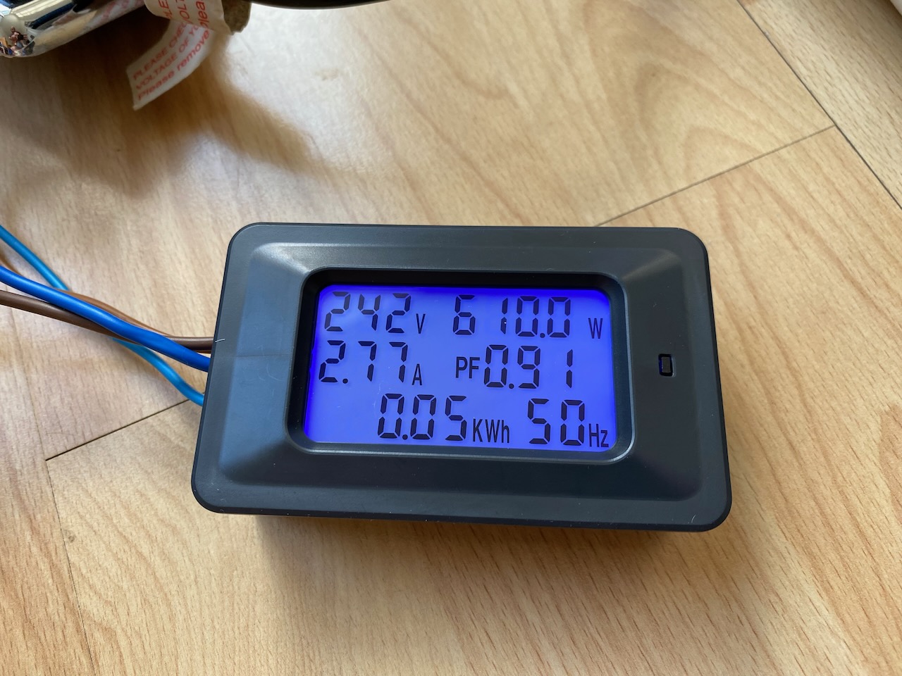
I wanted a visual indication that the inverter was on, and also some geeky statistics relating to the AC output. This power meter module from Amazon did the trick with its cheery blue backlight. It is powered from the AC supply, and this increases the 12V power draw of the inverter by about 1 watt.
A British Army F632 ammo box was procured to fit all the parts in and… they didn’t fit. To gain some extra space, I added a wooden frame to the front made from CLS studs. I am quite proud of the Stratocaster jack cups as PV input connectors.
I provided 3 DC outputs: two Powerpole connectors protected by 32A circuit breakers and a cigarette lighter with a 10A breaker. Household AC circuit breakers do seem to work on 12V DC. I’ve seen them used up to 48V DC.
The inverter feeds two British standard socket outlets via RCBOs (earth leakage trips). In order for these to function the inverter’s neutral is connected to earth. Battery negative is also connected to earth and in use the earth stud is connected to the container. I believe this is the best overall solution from an electrical safety point of view.
The RCBOs do consume some AC power to perform their earth leakage monitoring function, but the amount is tiny, and doesn’t increase the inverter standby consumption noticeably. I tried Axiom and British General brands, and the BG ones had the lowest consumption.
These also have a 6A overcurrent trip function (the O in RCBO) but the inverter’s own current limiting would probably always operate before they tripped.
The inverter was mounted on a plywood divider and some holes punched in the sides of the box to promote airflow. I also removed the AC socket outlet from the inverter, leaving a large square hole for extra airflow, cut out the fan grill from the inverter casing, and reversed the fan. Hopefully these changes will make up for jamming it inside a relatively small compartment.
To be honest I have no idea if reversing the fan helped the inverter’s own cooling. Stock behaviour is to suck hot air out of the enclosure, and the old rule of thumb is that it’s always better to blow in cooling systems, but the inverter seemed like a quite well balanced and optimised design otherwise, so I can’t believe the designers left much on the table with sub-optimal cooling.
Really it was for my own convenience at a system level, the fan is at the 12V input end of the inverter and I wanted the hot air exhaust at the opposite end to the battery terminals, so I could have shortest possible battery wiring and a neat “signal path” from DC to AC without the inverter’s hot air blowing onto the Victron charge controller.
You might notice the lack of fuses on the battery positive terminal. Every connection to the battery is ultimately protected by a fuse or circuit breaker, but not directly at the terminal.
In use, you can see the inputs from the PV panel and the earth wire leading to an earth clamp on the container. (A steel framed building as far as BS7671 is concerned I guess.) The 12V and 240V wiring are not done yet.
The power bank itself could also do with a coat of paint and some more industrial looking unswitched AC outlets. The chrome ones are a bit flashy. Weighing in at 45kg (perhaps Power Tank would be a more appropriate name?) it also needs some serious handles to assist in moving it around…
I love the way the meter backlights come on when the inverter switch is flipped.
Appliances the inverter has run successfully:
Toaster, obviously
1kW electric heater
400W “Eco Henry” vacuum cleaner
Clarke CDP102 pillar drill
Clarke 6″ bench grinder
1200W travel hair dryer (output sags to 220V, hair dryer only produces 1kW)
Ikea TILLREDA induction hotplate (only up to 40% power…)
A selection of guitar amps (works surprisingly well with no noise issues)