In 2011 I built the Selfless Amp, my first hifi power amp designed from scratch, albeit very strongly influenced by Douglas Self.
I also used it as an opportunity to try the then-new ThermalTrak power transistors from OnSemi. These have a temperature sensing diode co-packaged with the transistor, which promised to eliminate all biasing hassles.
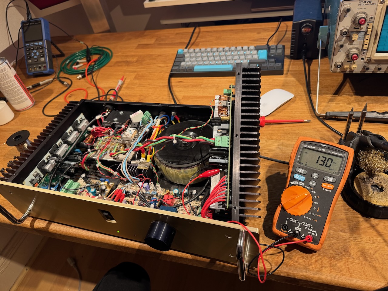
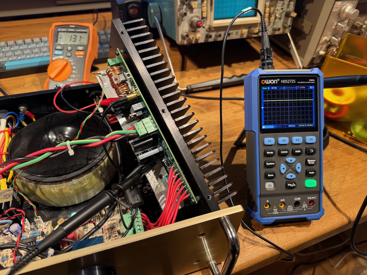
More recently I noticed the right channel heatsink was getting a lot hotter than the left channel. The problem would come and go, and a few times I reset the bias only for it to become too cold later.
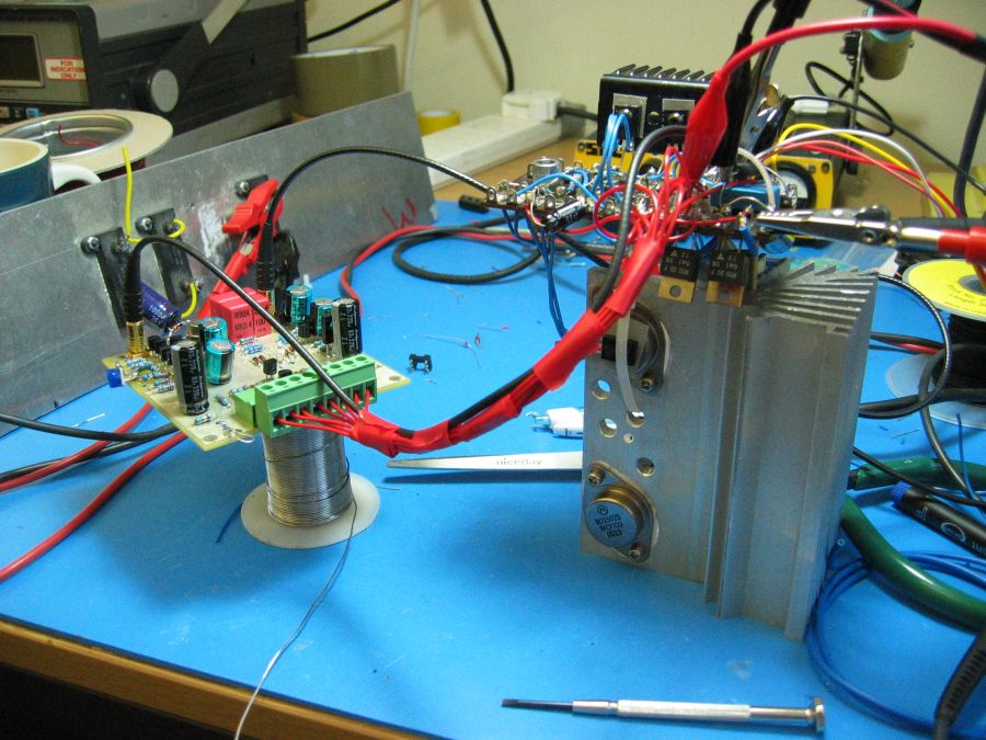
I ran it for ages like this but eventually got the time and inclination to get to the bottom of the issue. Prodding the circuitry with a stick and bending the circuit boards made no difference, so loose connections were ruled out. And the fault followed the output stage board when parts were swapped between channels. Therefore it was most likely either in the driver transistors, bias generator transistor, or one of the output devices.
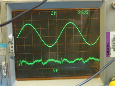
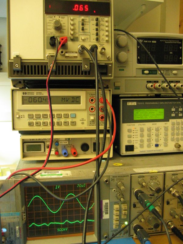
Connecting a scope in roll mode across one of the emitter resistors, I could see the quiescent current jumping around at random.

I tried replacing the driver and bias generator transistors (Q1 and Q3 in this schematic) but it made absolutely no difference. At this point I also noticed that the jumps in quiescent current could be seen across all of the emitter resistors. If the problem was in an output transistor, I’d expect it to only affect a single device.
This pretty much narrowed it down to an issue with the ThermalTrak diodes, so my next move was to replace Q4 and Q5, the pair of output devices whose diodes are used for bias generation.
Stability was restored.
I have seen faults like this in the past where semiconductor junctions would develop temperature sensitive behaviour over and above the usual -2 millivolt per kelvin. The late Bob Pease wrote about a batch of diodes he came across that acted as thermostats, going open circuit above a certain temperature. This seems to be a less extreme version of the same thing, where the forward voltage of the ThermalTrak diode jumps around at random by 10s of millivolts as the temperature ramps up. I’m an applications guy, not devices, so I don’t know the semiconductor physics behind it. My guess would be bad packaging putting a temperature dependent mechanical strain on the device.
The NJL4281/NJL4302 devices I used are end of life, but similar parts are still available.